NUI Galway – UL Alliance First Annual ENGINEERING AND - ARAN ...
NUI Galway – UL Alliance First Annual ENGINEERING AND - ARAN ...
NUI Galway – UL Alliance First Annual ENGINEERING AND - ARAN ...

You also want an ePaper? Increase the reach of your titles
YUMPU automatically turns print PDFs into web optimized ePapers that Google loves.
Interfacial strain analysis of Si, SiGe Strained-Layer Superlattice Structure<br />
using Convergent Beam Electron Diffraction<br />
N.V.V. Mogili 1, 2* , D.A. Tanner 1, 2 1, 3<br />
, S. Nakahara<br />
1 Materials & Surface Science Institute, University of Limerick, Ireland<br />
2 Department of Design and Manufacturing Technology, University of Limerick, Ireland<br />
3 Department of Physics & Energy, University of Limerick, Ireland<br />
Vishnu.Mogili@ul.ie<br />
Abstract<br />
Due to the mechanical thinning of Strained-Layer<br />
Superlattice (SLS) structure, two types of relaxation<br />
occur. One type of relaxation arises between adjacent<br />
layers of SLS and another between whole SLS and its<br />
substrate. In the present work by combining Low Angle<br />
Annular Dark Field (LAADF) imaging with Convergent<br />
Beam Electron Diffraction (CBED), the relaxation that<br />
appears between whole SLS and its substrate of Si,<br />
SiGe structure has been studied.<br />
Introduction<br />
Understanding the interfacial strain phenomenon of<br />
Strained-Layer Superlattices (SLS) and quantum well<br />
semiconductors at nanometer level is very important in<br />
designing advanced electronic devices. Due to the<br />
difference in lattice parameters of epitaxially grown<br />
materials, strain exists at adjacent layers of SLS and<br />
also between whole SLS and the substrate. The nature<br />
of the strain will be homogeneous when the SLS is in its<br />
bulk form. But as the complete structure is thinned<br />
down to electron transparency owing to elastic<br />
relaxation phenomenon, strain state will be altered. To<br />
quantitatively determine the local behavior of strain,<br />
Convergent Beam Electron Diffraction (CBED) is an<br />
excellent technique to study the layers of SLS with high<br />
spatial resolution.<br />
Material & Methods<br />
The specimen analyzed in this work is a TEM<br />
calibration sample known as MAG-I-CAL ® . It is a<br />
cross sectional SLS structure with alternating<br />
strained Silicon-Germanium (Si0.81Ge0.19) and Silicon<br />
(Si) layers grown epitaxially on Si substrate. CBED<br />
analysis was performed at a nominal voltage of 200kv in<br />
JEOL 2100 FEG TEM and all strain measurements were<br />
performed in [340] Zone Axis (ZA) which is 8° apart<br />
from [011] ZA.<br />
As the conical electron beam is used to illuminate the<br />
specimen surface, CBED patterns consists of pairs of<br />
deficit and excess High Order Laue Zone (HOLZ) lines<br />
appear in its transmitted and diffracted disks. The<br />
positions of these lines are very sensitive to the changes<br />
in local lattice parameters and Transmission Electron<br />
Microscope (TEM) accelerating voltage. Hence for the<br />
quantitative study of strain nature, initially TEM<br />
170<br />
accelerating voltage has been calculated with accuracy<br />
down to 0.05 kv by means of dynamical simulations<br />
using JEMS electron microscopy software. And for<br />
precise handling of electron beam on the specimen<br />
surface, CBED has been performed in Scanning<br />
Transmission Electron Microscope (STEM) mode.<br />
Results & Discussion<br />
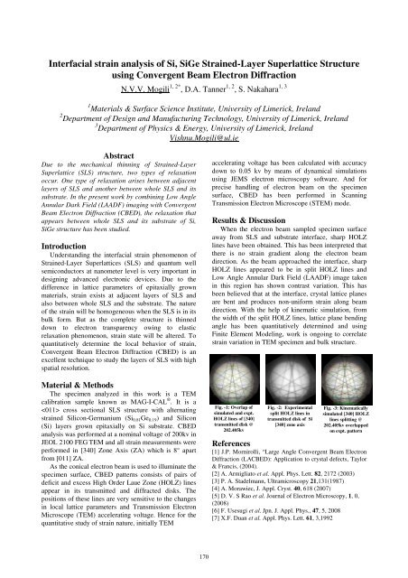
When the electron beam sampled specimen surface<br />
away from SLS and substrate interface, sharp HOLZ<br />
lines have been obtained. This has been interpreted that<br />
there is no strain gradient along the electron beam<br />
direction. As the beam approached the interface, sharp<br />
HOLZ lines appeared to be in split HOLZ lines and<br />
Low Angle Annular Dark Field (LAADF) image taken<br />
in this region has shown contrast variation. This has<br />
been believed that at the interface, crystal lattice planes<br />
are bent and produces non-uniform strain along beam<br />
direction. With the help of kinematic simulation, from<br />
the width of the split HOLZ lines, lattice plane bending<br />
angle has been quantitatively determined and using<br />
Finite Element Modeling, work is ongoing to correlate<br />
strain variation in TEM specimen and bulk structure.<br />
Fig. -1: Overlap of<br />
simulated and expt.<br />
HOLZ lines of [340]<br />
transmitted disk @<br />
202.405kv<br />
Fig. -2: Experimental<br />
split HOLZ lines in<br />
transmitted disk of Si<br />
[340] zone axis<br />
Fig. -3: Kinematically<br />
simulated [340] HOLZ<br />
lines splitting @<br />
202.405kv overlapped<br />
on expt. pattern<br />
References<br />
[1] J.P. Mornirolli, “Large Angle Convergent Beam Electron<br />
Diffraction (LACBED): Application to crystal defects, Taylor<br />
& Francis, (2004).<br />
[2] A. Armigliato et al. Appl. Phys. Lett. 82, 2172 (2003)<br />
[3] P. A. Stadelmann, Ultramicroscopy 21,131(1987)<br />
[4] A. Morawiec, J. Appl. Cryst. 40, 618 (2007)<br />
[5] D. V. S Rao et al. Journal of Electron Microscopy, 1, 0,<br />
(2008)<br />
[6] F. Usesugi et al. Jpn. J. Appl. Phys., 47, 5, 2008<br />
[7] X.F. Duan et al. Appl. Phys. Lett. 61, 3,1992