PDP11 PeripheralsHbk 1972 - Trailing-Edge
PDP11 PeripheralsHbk 1972 - Trailing-Edge
PDP11 PeripheralsHbk 1972 - Trailing-Edge

You also want an ePaper? Increase the reach of your titles
YUMPU automatically turns print PDFs into web optimized ePapers that Google loves.
2.2.6 M795 Word Count and Bus· Address Module<br />
The M795 Word Count and Bus address Module is used to interface direct<br />
memory access (OMA) devices to the UNIBUS. This module contains two 16·bit<br />
counters: one counter is used to count the number of data transfers that occur;<br />
the other counter is used to specify the bus address of the data to be transferred.<br />
Block transfer devices that function as bus master during data transfers usually<br />
require two registers to hold the parameters of the transfer. One parameter is<br />
transfer count. Initially, a register is loaded with, the 2's complement of the num·<br />
ber of items to be transferred to or from memory. After each transfer is complete,<br />
the register is incremented. If the new value of the register is 0 (indicated by an<br />
overflow), further transfers are inhibited and the block transfer is complete. Since<br />
information can be transferred in words (16 bits each) on the UNIBUS the name<br />
Word Count (WC) is usually assigned to this register. However, the UNIBUS is<br />
also capable of transferring 8·bit bytes of data at a time, and this register may be<br />
used equally as well as a Byte Count register.<br />
The second parameter used in block transfers is the transfer address. Initially, a<br />
register is loaded with an address that specifies the memory location to, or from,<br />
which data is to be transferred. The register is incremented after each transfer;<br />
thus, the register continually "points" to sequential memory locc;ltions. Since<br />
memories and devices have addresses on the UNIBUS, this register is usually<br />
called the Bus address (BA) register.<br />
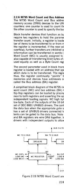
A simplified block diagram of the M795 module is shown in Figure 2·19. Both the<br />
word count (WC) and bus address (BA) registers consist of 16 flip·flops. These<br />
flip·flop registers can be loaded by placing data on the 16 data line inputs com·<br />
man to both registers and asserting the appropriate loading signal. There are four<br />
independent loading signals: WC high byte, WC low byte, BA high byte, and BA<br />
low byte. Each of the outputs of the 16 bits in the WC register are connected to a<br />
set of DEC 8881 UN IBUS drivers. The contents of the WC register can be gated to<br />
the data bus when the appropriate gate signal is activated. The BA register also<br />
has a set of UN IBUS drivers connected to each output so that the register con·<br />
tents can be gated to the data bus. Note that the driver outputs of both the WC<br />
and BA registers are wire ORd together. In addition, the BA register has a set of<br />
drivers with independent outputs to allow it to drive the address bus.<br />
WC OVFL<br />
LOAD WC<br />
LOAD WC+l<br />
COUNT SA<br />
Figure 2-19 M795 Word Count and Bus Address (block diagram)<br />
224