PDP11 PeripheralsHbk 1972 - Trailing-Edge
PDP11 PeripheralsHbk 1972 - Trailing-Edge
PDP11 PeripheralsHbk 1972 - Trailing-Edge

Create successful ePaper yourself
Turn your PDF publications into a flip-book with our unique Google optimized e-Paper software.
nel and low COY) for a transfer from the channel; a break state (BRK STATE) signal,<br />
which is low when the secondary computer is in the break state; and three<br />
timing signals transmitted by the channel control to indicate break and address<br />
accepted (BRK ACPT), data accepted (DATA ACPT), and data available (DATA<br />
AVAil).<br />
3.7.2 Interface Description<br />
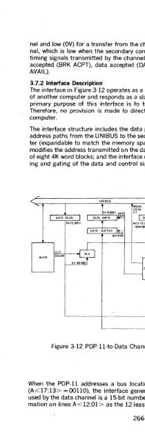
The interface in Figure 3-12 operates as a cycle stealing device on a data channel<br />
of another computer and responds as a slave device on the PDP-11 UNIBUS. The<br />
primary purpose of this interface is to transfer data between two processors.<br />
Therefore, no provision is made to directly control operation of the secondary<br />
computer.<br />
The interface structure includes the data paths between the two processors; the<br />
address paths from the UNIBUS to the secondary processor; a block (BLK) register<br />
(expandable to match the memory space of the secondary processor), which<br />
modifies the address transmitted on the data channel in order for it to access one<br />
of eight 4K word blocks; and the interface control logic, which determines the timing<br />
and gating of the data and control signal flow.<br />
M105<br />
elK<br />
DCCSR<br />
OATA OUT<br />
r------l<br />
I<br />
I<br />
I<br />
I<br />
figure 3-12 PDP-11-to-Data Channel Interface (block diagram)<br />
When the PDP-11 addresses a bus location in the seventh block of 4K words<br />
(A =00110), the interface generates a BRK REQ signal. The address<br />
used by the data channel is a 15-bit number assembled by transmitting the informationon<br />
lines A < 12:01 > as the 12 least significant bits, and transmitting the<br />
266