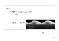
Effect of Post Metallization Annealing for La 2 O 3 Thin Film
Effect of Post Metallization Annealing for La 2 O 3 Thin Film
Effect of Post Metallization Annealing for La 2 O 3 Thin Film

Create successful ePaper yourself
Turn your PDF publications into a flip-book with our unique Google optimized e-Paper software.
1.1.3 Requirements <strong>for</strong> High-k Gate DielectricsThe reason to thin down SiO2 is to increase gate charges, whichincreases drain current. The capacitance Ci <strong>of</strong> gate dielectric at unit area isexpressed with the following equation,Cε kt0i= (1.1)where ε0and k are vacuum and relative dielectric constant, respectivelyand t is the thickness <strong>of</strong> gate dielectrics. The value <strong>of</strong> vacuum dielectricconstant is about 8.85× 10 −14 [F/cm] and relative dielectric constant <strong>of</strong> SiO2 is3.9. <strong>Thin</strong>ning down SiO2 used to be a simple and effective way to obtainhigh capacitance value as SiO2 is greatly stable with silicon substrates asmentioned in <strong>for</strong>mer section. Now that the limit <strong>of</strong> SiO2 is showing up,however, another way to increase the capacitance value is required. Theanswer <strong>for</strong> this requirement is to introduce new materials which have highdielectric constant. These materials are called high-k dielectrics. If onematerial which have a dielectric constant, k=7.8 (double compared to SiO2)can be replaced instead <strong>of</strong> SiO2, the capacitance value is maintained eventhough thickness <strong>of</strong> gate insulator become twice. If this replacement can bepossible, that will be the answer enough to prevent direct tunneling effecttaking place shown in Figure 1-4.It is, however, not simple to replace SiO2 to the high-k materials,because the high-k dielectrics must satisfy several conditions whichdetermine the electrical properties <strong>of</strong> MOSFET. The requirements <strong>for</strong>high-k dielectrics are described in the pages that follow.(1) High dielectric constantAs is already mentioned, the higher dielectric constant is, the thickerthe gate insulator can be <strong>for</strong> same capacitance value. At the same time,however, the band gap which determines the barrier height against electronsand holes is roughly inversely proportional to the dielectric constant.There<strong>for</strong>e, it is necessary <strong>for</strong> high-k dielectrics to be compatible with theband gap in order to suppress the leakage currents due to Schottky emission.Generally, it is considered that dielectric constant less than 50 is desirable.(2) Stability at high thermal condition in contact with Si surfaceThere are some processes with thermal condition around 1000K in-6 -