Effect of Post Metallization Annealing for La 2 O 3 Thin Film
Effect of Post Metallization Annealing for La 2 O 3 Thin Film
Effect of Post Metallization Annealing for La 2 O 3 Thin Film

You also want an ePaper? Increase the reach of your titles
YUMPU automatically turns print PDFs into web optimized ePapers that Google loves.
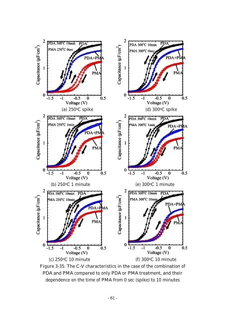
Capacitance (µF/cm 2 )21PDA 300 o C 10minPMA 250 o C 0secPDAPDA+PMAPMACapacitance (µF/cm 2 )21PDA 300 o C 10minPMA 300 o C 0secPDAPDA+PMAPMACapacitance (µF/cm 2 )0-1.5 -1 -0.5 0 0.5Voltage (V)(a) 250 o C spike2PDA 300 o C 10minPDAPMA 250 o C 1minPDA+PMA1PMACapacitance (µF/cm 2 )0-1.5 -1 -0.5 0 0.5Voltage (V)(d) 300 o C spike2PDAPDA 300 o C 10minPMA 300 o C 1minPDA+PMA1PMACapacitance (µF/cm 2 )0-1.5 -1 -0.5 0 0.5Voltage (V)(b) 250 o C 1 minute2PDA 300 o C 10minPDAPMA 250 o C 10minPDA+PMA1PMACapacitance (µF/cm 2 )0-1.5 -1 -0.5 0 0.5Voltage (V)(e) 300 o C 1 minute2PDA 300 o C 10minPDAPMA 300 o C 10minPDA+PMA1PMA00-1.5 -1 -0.5 0 0.5-1.5 -1 -0.5 0 0.5Voltage (V)Voltage (V)(c) 250 o C 10 minute(f) 300 o C 10 minuteFigure 3-35: The C-V characteristics in the case <strong>of</strong> the combination <strong>of</strong>PDA and PMA compared to only PDA or PMA treatment, and theirdependence on the time <strong>of</strong> PMA from 0 sec (spike) to 10 minutes- 61 -