Effect of Post Metallization Annealing for La 2 O 3 Thin Film
Effect of Post Metallization Annealing for La 2 O 3 Thin Film
Effect of Post Metallization Annealing for La 2 O 3 Thin Film

You also want an ePaper? Increase the reach of your titles
YUMPU automatically turns print PDFs into web optimized ePapers that Google loves.
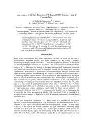
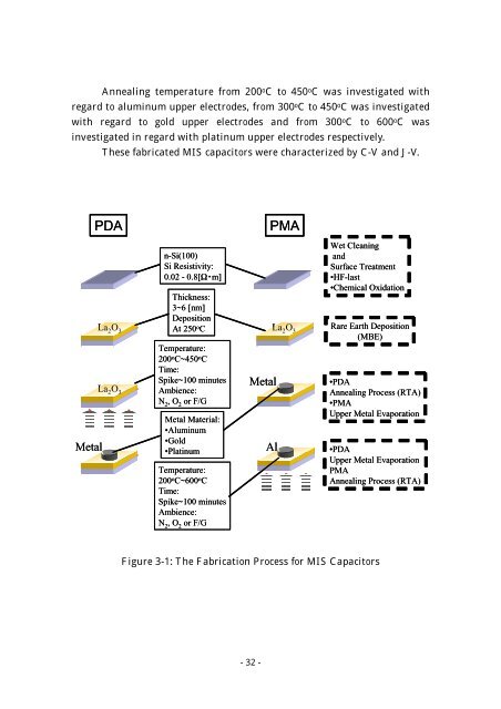
<strong>Annealing</strong> temperature from 200 o C to 450 o C was investigated withregard to aluminum upper electrodes, from 300 o C to 450 o C was investigatedwith regard to gold upper electrodes and from 300 o C to 600 o C wasinvestigated in regard with platinum upper electrodes respectively.These fabricated MIS capacitors were characterized by C-V and J-V.MetalPDAPMAn-Si(100)Si Resistivity:0.02 - 0.8[Ω・m]Thickness:3~6 [nm]<strong>La</strong> 2 O 3 DepositionAt 250 o C<strong>La</strong> 2 O 3Temperature:200 o C~450 o CTime:Spike~100 minutes<strong>La</strong> 2 O 3Ambience:N 2 , O 2 or F/GMetal Material:•Aluminum•Gold•PlatinumTemperature:200 o C~600 o CTime:Spike~100 minutesAmbience:N 2 , O 2 or F/GMetalAlWet CleaningandSurface Treatment•HF-last•Chemical OxidationRare Earth Deposition(MBE)•PDA<strong>Annealing</strong> Process (RTA)•PMAUpper Metal Evaporation•PDAUpper Metal EvaporationPMA<strong>Annealing</strong> Process (RTA)Figure 3-1: The Fabrication Process <strong>for</strong> MIS Capacitors- 32 -