Effect of Post Metallization Annealing for La 2 O 3 Thin Film
Effect of Post Metallization Annealing for La 2 O 3 Thin Film
Effect of Post Metallization Annealing for La 2 O 3 Thin Film

You also want an ePaper? Increase the reach of your titles
YUMPU automatically turns print PDFs into web optimized ePapers that Google loves.
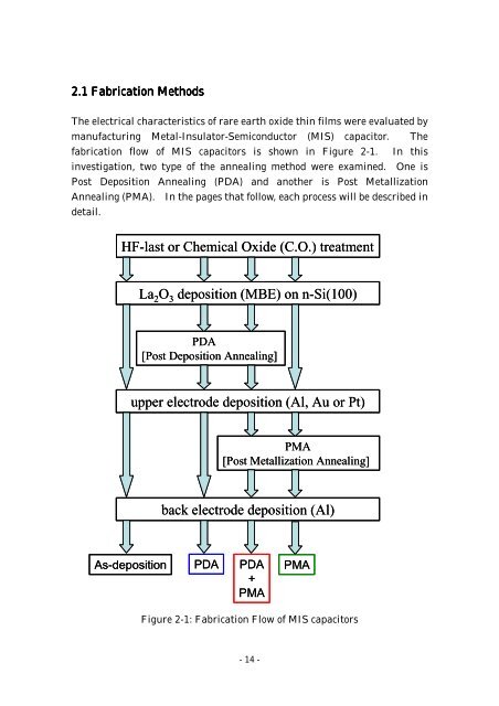
2.1 Fabrication MethodsThe electrical characteristics <strong>of</strong> rare earth oxide thin films were evaluated bymanufacturing Metal-Insulator-Semiconductor (MIS) capacitor. Thefabrication flow <strong>of</strong> MIS capacitors is shown in Figure 2-1. In thisinvestigation, two type <strong>of</strong> the annealing method were examined. One is<strong>Post</strong> Deposition <strong>Annealing</strong> (PDA) and another is <strong>Post</strong> <strong>Metallization</strong><strong>Annealing</strong> (PMA). In the pages that follow, each process will be described indetail.HF-last or Chemical Oxide (C.O.) treatment<strong>La</strong> 2 O 3 deposition (MBE) on n-Si(100)PDA[<strong>Post</strong> Deposition <strong>Annealing</strong>]upper electrode deposition (Al, Au or Pt)PMA[<strong>Post</strong> <strong>Metallization</strong> <strong>Annealing</strong>]back electrode deposition (Al)As-deposition PDA PDA+PMAPMAFigure 2-1: Fabrication Flow <strong>of</strong> MIS capacitors- 14 -