Effect of Post Metallization Annealing for La 2 O 3 Thin Film
Effect of Post Metallization Annealing for La 2 O 3 Thin Film
Effect of Post Metallization Annealing for La 2 O 3 Thin Film

Create successful ePaper yourself
Turn your PDF publications into a flip-book with our unique Google optimized e-Paper software.
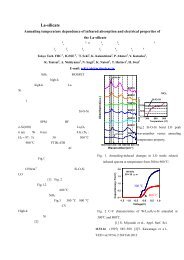
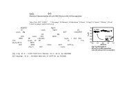
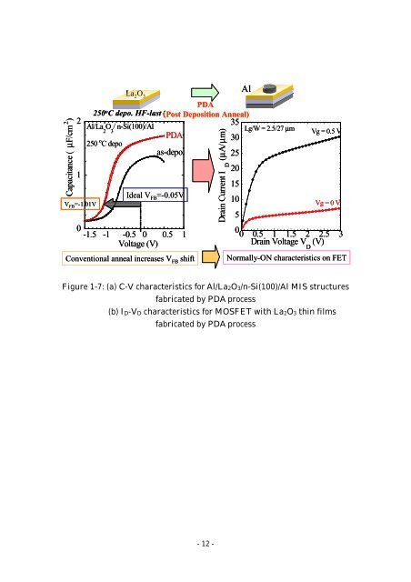
<strong>La</strong> 2 O 3PDA250 o C depo. HF-last(<strong>Post</strong> Deposition Anneal)235Al/<strong>La</strong> O / n-Si(100)/Al2 3 Lg/W = 2.5/27 µmPDA30250 o C depoas-depo.2520115Ideal V FB =-0.05V10V FB =-1.01V5Capacitance ( µF/cm 2 )0-1.5 -1 -0.5 0 0.5 1Voltage (V)Conventional anneal increases V FB shiftDrain Current I D (µA/µm)AlVg = 0.5 VVg = 0 V00 0.5 1 1.5 2 2.5 3Drain Voltage V (V)D Normally-ON characteristics on FETFigure 1-7: (a) C-V characteristics <strong>for</strong> Al/<strong>La</strong>2O3/n-Si(100)/Al MIS structuresfabricated by PDA process(b) ID-VD characteristics <strong>for</strong> MOSFET with <strong>La</strong>2O3 thin filmsfabricated by PDA process- 12 -