Effect of Post Metallization Annealing for La 2 O 3 Thin Film
Effect of Post Metallization Annealing for La 2 O 3 Thin Film
Effect of Post Metallization Annealing for La 2 O 3 Thin Film

Create successful ePaper yourself
Turn your PDF publications into a flip-book with our unique Google optimized e-Paper software.
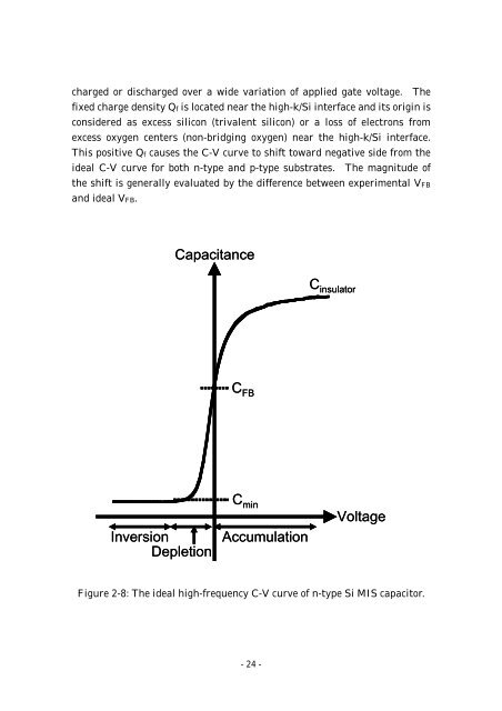
charged or discharged over a wide variation <strong>of</strong> applied gate voltage. Thefixed charge density Qf is located near the high-k/Si interface and its origin isconsidered as excess silicon (trivalent silicon) or a loss <strong>of</strong> electrons fromexcess oxygen centers (non-bridging oxygen) near the high-k/Si interface.This positive Qf causes the C-V curve to shift toward negative side from theideal C-V curve <strong>for</strong> both n-type and p-type substrates. The magnitude <strong>of</strong>the shift is generally evaluated by the difference between experimental VFBand ideal VFB.CapacitanceC insulatorC FBInversionDepletionC minAccumulationVoltageFigure 2-8: The ideal high-frequency C-V curve <strong>of</strong> n-type Si MIS capacitor.- 24 -