IGCAR : Annual Report - Indira Gandhi Centre for Atomic Research
IGCAR : Annual Report - Indira Gandhi Centre for Atomic Research
IGCAR : Annual Report - Indira Gandhi Centre for Atomic Research

Create successful ePaper yourself
Turn your PDF publications into a flip-book with our unique Google optimized e-Paper software.
IGC<br />
<strong>Annual</strong> <strong>Report</strong> 2007<br />
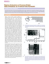
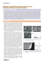
Fig.2 Timing spectrum<br />
mm thick NaI(Tl) crystal<br />
coupled with 203 mm, 50 mm<br />
CsI(Tl) crystal and optically<br />
coupled to three matched 3"<br />
dia photomultiplier tubes (ETL<br />
9255). The detector has an<br />
ultra low background 0.5 mm<br />
thick beryllium entrance<br />
window. The new PSD, based<br />
on scintillation time<br />
comparison, uses the rise time<br />
difference in the signals of<br />
NaI(Tl) (250 ns) and CsI(Tl)<br />
(1100 ns) to produce a gating<br />
pulse to selectively choose the<br />
pulses due to LE photon<br />
interactions in NaI(Tl) alone.<br />
The schematic of the PSD<br />
electronics with typical signals<br />
is shown in Fig.1.<br />
The Pulse Shape Analyser<br />
(PSA), analyses the input pulses<br />
and generates two negative<br />
pulses, one at 90% peak<br />
amplitude labeled as "A" and<br />
another at selected fraction (B)<br />
of the peak amplitude labeled<br />
as "B". The outputs "A" and "B"<br />
from PSA are fed to the inputs<br />
of Time to Amplitude Converter<br />
(TAC) as "Start" and "Stop"<br />
pulses, respectively. This results<br />
in TAC unit generating a square<br />
pulse whose amplitude is<br />
proportional to the time<br />
difference between A & B.<br />
Hence, the LE photon<br />
interaction from NaI(Tl)<br />
generates pulses with lower<br />
amplitudes compared to the<br />
pulses from CsI(Tl). Once the<br />
amplitude of TAC pulses<br />
corresponding to NaI(Tl) or CsI<br />
is known, any of them can be<br />
selected <strong>for</strong> gating by using a<br />
SCA with properly selected LLD<br />
& ULD.<br />
Processing of pulses <strong>for</strong><br />
risetime analysis results a time<br />
delay in generating gate pulse.<br />
Typical time delay is observed<br />
to be 3.75 µs <strong>for</strong> NaI(Tl) pulses<br />
and 5.75 µs <strong>for</strong> CsI pulses.<br />
Every bipolar pulse from delay<br />
line amplifier is precisely<br />
delayed and then presented to<br />
MCA <strong>for</strong> analysis. One of the<br />
inputs of MCA coincidence<br />
circuit is the delayed pulse from<br />
delay amplifier and the other<br />
input is the gating pulse from<br />
the SCA. The input pulses to the<br />
delay amplifier are accepted<br />
<strong>for</strong> spectrum analysis only when<br />
the gating pulses occur<br />
simultaneously. This results in<br />
rejection of most of the<br />
unwanted high energy<br />
interactions, which will have a<br />
time characteristic of CsI(Tl)<br />
detector, thereby reducing the<br />
background considerably.<br />
The timing spectrum obtained<br />
with 137Cs source, with<br />
optimized PSD parameters, is<br />
shown in Fig.2. The figure of<br />
merit (M) <strong>for</strong> the obtained<br />
timing spectrum is estimated to<br />
be 3.0.<br />
Comparison of the peak<br />
position and the FWHM values<br />
obtained <strong>for</strong> 17 keV, 60 keV<br />
and 122 keV with and without<br />
PSD electronics clearly shows<br />
that PSD has not affected<br />
spectrum parameters. In order<br />
to quantitatively estimate the<br />
background reduction, spectra<br />
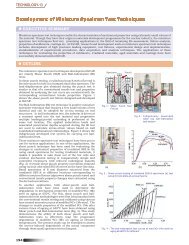
were obtained with and without<br />
PSD (Figure-3). The inclusion of<br />
PSD electronics has reduced<br />
the background from 9.5 cps to<br />
0.28 cps in 17 keV region and<br />
5.8 cps to 0.3 cps in 60 keV<br />
region. This results in an<br />
improvement in the MDA values<br />
by a factor of 2.<br />
A state of art pulse shape<br />
discriminator employing readily<br />
available nuclear electronics<br />
Fig.3 Background reduction with<br />
PSD electronics<br />
ENABLING TECHNOLOGIES 133