IGCAR : Annual Report - Indira Gandhi Centre for Atomic Research
IGCAR : Annual Report - Indira Gandhi Centre for Atomic Research
IGCAR : Annual Report - Indira Gandhi Centre for Atomic Research

Create successful ePaper yourself
Turn your PDF publications into a flip-book with our unique Google optimized e-Paper software.
IGC<br />
<strong>Annual</strong> <strong>Report</strong> 2007<br />
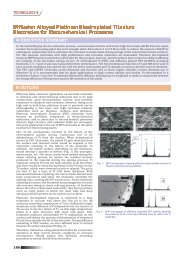
rising partial pressure of<br />
nitrogen gas was maintained.<br />
The compositional depth profile<br />
of this multilayer architecture<br />
was analyzed by Secondary Ion<br />
Mass Spectrometry (SIMS) using<br />
Cs + primary ion beam. The Cs<br />
Ti + and CsN 2+<br />
quasimolecular<br />
complexes were monitored<br />
along with CsO + and CsSi + to<br />
get the compositional variation<br />
as a function of sputter depth.<br />
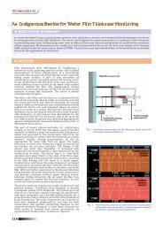
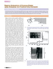
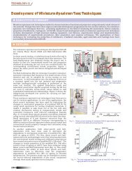
Fig. 2 shows the composition<br />
depth profiles <strong>for</strong> the elements<br />
Ti, Si, N and O. The N/Ti ratio<br />
increases with increase in<br />
deposition pressure from 5.0 ×<br />
10 -5 mbar, reaches a maximum<br />
<strong>for</strong> films deposited at<br />
5.0 × 10 -2 mbar and then<br />
declines owing to the<br />
preponderance of O 2 at higher<br />
Fig.2 SIMS depth profile of TiN multilayers grown sequentialy on Si<br />
substrate at various deposition pressures by RPLD<br />
Fig.3 High Resolution TEM image of the RPLD grown TiN film<br />
(Insert A) elasto-plastic de<strong>for</strong>mation profile obtained by<br />
nano-indentation (Insert B) selected area electron diffraction pattern<br />
pressures. Thus it can be<br />
concluded that the deposition<br />
pressure of ~10 -2 mbar is the<br />
optimal condition <strong>for</strong> growing<br />
stoichiometric nanostructured<br />
TiN coatings.<br />
The high resolution TEM<br />
image of the TiN film grown on<br />
a NaCl substrate at 2 × 10 -2<br />
mbar and the corresponding<br />
Selected Area Electron<br />
Diffraction (SAED) pattern is<br />
shown in figure 3. These studies<br />
indicated the <strong>for</strong>mation of films<br />
highly oriented in the <br />
and directions. The d-<br />
spacing calculated from the<br />
diffraction pattern matches well<br />
with the literature values<br />
reported in PCPDF data. A<br />
typical nanoindentation profile<br />
of 800 nm thick TiN film coated<br />
on silicon substrate at<br />
2.0× 10 -2 mbar is shown as an<br />
inset in the high resolution TEM<br />
m i c r o s t r u c t u r e .<br />
Nanoindentation studies of thin<br />
films, are aimed at providing<br />
better interpretations of the<br />
elastic modulus, yield strength,<br />
strain hardening and hardness<br />
of the surface only. The<br />
hardness and modulus of the<br />
film at a depth of 80 nm<br />
calculated from the loading<br />
and unloading profile using<br />
Oliver-Pharr technique is 20<br />
GPa and 231 GPa, respectively.<br />
Ef<strong>for</strong>ts are on to synthesize AlN,<br />
ZrN and NbN coatings in<br />
similar way with an aim to<br />
produce multilayered<br />
nanostructured films with<br />
heterolaminate architecture.<br />
150 BASIC RESEARCH