- Page 1 and 2:
Laboratory Directed Research and De
- Page 3 and 4:
Laboratory Directed Research and De
- Page 5 and 6:
Computational Science and Engineeri
- Page 7 and 8:
Policy and Management Sciences Asse
- Page 9 and 10:
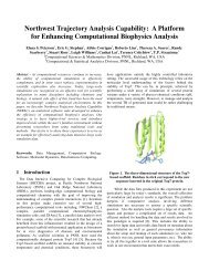
Introduction Department of Energy O
- Page 11 and 12:
5. After reviews by the Technical a
- Page 13 and 14:
• The Technical Council peer revi
- Page 15 and 16:
methods applicable to combustion, s
- Page 17 and 18:
Summary Each national laboratory mu
- Page 19 and 20:
Study Control Number: PN0004/1411 A
- Page 21 and 22:
Table 1. Positive and negative ions
- Page 23 and 24:
m/z Arbitrary Units Figure 1. Mass
- Page 25 and 26:
introduce low-volatility compounds
- Page 27 and 28:
arrangement, but the charge is reta
- Page 29 and 30:
two liquid chromatographic gradient
- Page 31 and 32:
Integrated Microfabricated Devices
- Page 33 and 34:
Matrix Assisted Laser Desorption/Io
- Page 35 and 36:
Molecular Beam Synthesis and Charac
- Page 37 and 38:
temperature distribution of the des
- Page 39 and 40:
expected to result in significant a
- Page 41 and 42:
Study Control Number: PN99069/1397
- Page 43 and 44:
Study Control Number: PN99073/1401
- Page 45 and 46:
Seuss DT and KA Prather. 1999. “M
- Page 47 and 48:
Analysis of Receptor-Modulated Ion
- Page 49 and 50:
laboratory (Lu and Xie 1997; Lu et
- Page 51 and 52:
Automated DNA Fingerprinting Microa
- Page 53 and 54:
Comparison of 4 Xanthomonas Isolate
- Page 55 and 56:
Approach Hematopoietic (bone marrow
- Page 57 and 58:
Study Control Number: PN99005/1333
- Page 59 and 60:
Anti-Human lgG Human lgG Protein G
- Page 61 and 62:
Characterization of Global Gene Reg
- Page 63 and 64:
PCR products for immobilization on
- Page 65 and 66:
identify novel proteins of importan
- Page 67 and 68:
Immunoprecipitaton of tyrosinephosp
- Page 69 and 70:
Coupled NMR and Confocal Microscopy
- Page 71 and 72:
In the optical microscopy image, th
- Page 73 and 74:
Development and Applications of a M
- Page 75 and 76:
Figure 3. Hepa-1 cells undergoing a
- Page 77 and 78:
cellular processing (such as post-t
- Page 79 and 80:
8. Initial demonstration of an off-
- Page 81 and 82:
expression systems for several year
- Page 83 and 84:
accumulation of protein products, i
- Page 85 and 86:
Study Control Number: PN00039/1446
- Page 87 and 88:
Fungal Conversion of Agricultural W
- Page 89 and 90:
Fungal Conversion of Waste Glucose/
- Page 91 and 92:
Summary and Conclusions We demonstr
- Page 93 and 94:
are shown in Figure 1(a) and 1(b),
- Page 95 and 96:
Study Control Number: PN99029/1357
- Page 97 and 98:
Study Control Number: PN99036/1364
- Page 99 and 100:
Anchorage-Independent Growth (% con
- Page 101 and 102:
selection of seedlings demonstratin
- Page 103 and 104:
NMR-Based Structural Genomics Micha
- Page 105 and 106:
Solution-State Structure and Fold-C
- Page 107 and 108:
Plant Root Exudates and Microbial G
- Page 109 and 110:
98 99 100 6 7 10 3 1 12 11 15 16 17
- Page 111 and 112:
Study Control Number: PN00077/1484
- Page 113 and 114:
Study Control Number: PN99064/1392
- Page 115 and 116:
Summary and Conclusions • The gre
- Page 117 and 118:
Study Control Number: PN00021/1428
- Page 119 and 120:
Jones-Oliveira JB, JS Oliveira, HE
- Page 121 and 122:
• securely moves files to a targe
- Page 123 and 124:
Study Control Number: PN98013/1259
- Page 125 and 126:
Plenary invited lecture, “The Ele
- Page 127 and 128:
Figure 1. X3DGEN tetrahedral mesh o
- Page 129 and 130:
Figure 5a. OSO volume rendering of
- Page 131 and 132:
Development of Models of Cell-Signa
- Page 133 and 134:
SOS p 23 EGFR Professor Rodland at
- Page 135 and 136:
Oliveira JS, JB Jones-Oliveira, and
- Page 137 and 138:
Figure 2. Associating a dataset mar
- Page 139:
to 1) incorporate three-dimensional
- Page 142 and 143:
shown in Figure 1. Simulated result
- Page 144 and 145:
HostBuilder: A Tool for the Combina
- Page 146 and 147:
Invariant Discretization Methods fo
- Page 148 and 149:
Graphics, Inc., workstation. The co
- Page 150 and 151:
Study Control Number: PN00063/1470
- Page 152 and 153:
Mixed Hamiltonian Methods for Geoch
- Page 154 and 155:
guyanaite, and grimaldiite (see Fig
- Page 156 and 157:
in the Environmental Molecular Scie
- Page 158 and 159:
Simulation and Modeling of Electroc
- Page 160 and 161:
Summary and Conclusions We implemen
- Page 162 and 163:
Study Control Number: PN00003/1410
- Page 164 and 165:
Since the implementation of the gen
- Page 166 and 167:
asis of previous performance, perce
- Page 168 and 169:
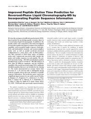
Bioinformatics for High-Throughput
- Page 170 and 171:
Summary and Conclusions In previous
- Page 172 and 173:
User Cat - Supervisor (client) Anal
- Page 174 and 175:
The second goal was to research way
- Page 176 and 177:
Figure 1. A visualization technique
- Page 178 and 179:
and interactions. The flexibility o
- Page 180 and 181:
Study Control Number: PN00085/1492
- Page 182 and 183:
Study Control Number: PN99078/1406
- Page 184 and 185:
Figure 4. A filtered version of Fig
- Page 186 and 187:
Development of Modeling Tools for J
- Page 188 and 189:
Figure 2. Schematic of experimental
- Page 190 and 191:
Integrated Modeling and Simulation
- Page 192 and 193:
(a) (b) (c) (d) Figure 1. Results o
- Page 194 and 195:
Thurman DA. August 2000. Collaborat
- Page 196 and 197:
MARC Input initial m esh and result
- Page 198 and 199:
(Johnson 1999; Colligan 1999; Gould
- Page 200 and 201:
Modeling of High-Velocity Forming f
- Page 202 and 203:
Global divergence error 1 10 -14 0
- Page 204 and 205:
that users were unlikely to appreci
- Page 206 and 207:
Earth System Science
- Page 208 and 209:
the lateral extent of the plume so
- Page 210 and 211:
Biogeochemical Processes and Microb
- Page 212 and 213:
Analyses of populations of viable a
- Page 214 and 215:
The first task was to establish fiv
- Page 216 and 217:
purged for 2 minutes. The gas sampl
- Page 218 and 219:
developing code architecture to min
- Page 220 and 221:
Berkowitz, CM. June 2000. “Atmosp
- Page 222 and 223:
environmental monitoring, 2) portab
- Page 224 and 225:
corresponded to a current density o
- Page 226 and 227:
Enhancing Emissions Pre-Processing
- Page 228 and 229:
Environmental Fate and Effects of D
- Page 230 and 231:
nitrogen and unpredictable eutrophi
- Page 232 and 233:
Figure 1. Ordinary kriging of 2 m d
- Page 234 and 235:
Study Control Number: PN00053/1460
- Page 236 and 237:
precipitation of calcite occurred i
- Page 238 and 239:
Study Control Number: PN00054/1461
- Page 240 and 241:
Interrelationships Between Processe
- Page 242 and 243:
phenanthrene resistant fraction con
- Page 244 and 245:
injection of an immiscible gas phas
- Page 246 and 247:
still some key kinetic issues that
- Page 248 and 249:
Study Control Number: PN99059/1387
- Page 250 and 251:
Application of a Crop Model The res
- Page 252 and 253:
The Nature, Occurrence, and Origin
- Page 254 and 255:
Particle number concentration, 1/cm
- Page 256 and 257:
geometry optimized AlOOH and FeOOH
- Page 258 and 259:
Study Control Number: PN00088/1495
- Page 260 and 261:
allowable parameters using thermody
- Page 262 and 263:
TCE + 3H + + 3Fe 2+ Fe)=> acetylene
- Page 264 and 265:
Use of Shear-Thinning Fluids for In
- Page 266 and 267:
concentration of 0.5% AMX was the m
- Page 268 and 269:
Roberts AL, LA Totten, WA Arnold, D
- Page 270 and 271:
tetra-scale computing, envisioned a
- Page 272 and 273:
Study Control Number: PN99079/1407
- Page 274 and 275:
Energy Technology and Management
- Page 276 and 277:
Figure 2. Setup for the second expe
- Page 278 and 279:
phase. The algorithms will be teste
- Page 280 and 281:
Study Control Number: PN00001/1408
- Page 282 and 283:
[Pb-212]/[Pb-212] final 100 10 1 0.
- Page 284 and 285:
Plasma Particle Dielectric Fiber El
- Page 286 and 287:
(species, sub-species, and sex), sp
- Page 288 and 289:
Figure 3. Relative risk of bone and
- Page 290 and 291:
Development of a Preliminary Physio
- Page 292 and 293:
Development of a Virtual Respirator
- Page 294 and 295: Figure 3. Use of the chest cavity a
- Page 296 and 297: Examination of the Use of Diazolumi
- Page 298 and 299: Indoor Air Pathways to Nuclear, Che
- Page 300 and 301: Source Building Release Observed re
- Page 302 and 303: To illustrate the potential impact
- Page 304 and 305: Non-Invasive Biological Monitoring
- Page 306 and 307: Study Control Number: PN00079/1486
- Page 308 and 309: Materials Science and Technology
- Page 310 and 311: Figure 1. (a) - (c) Successive magn
- Page 312 and 313: Component Fabrication and Assembly
- Page 314 and 315: Development of a Low-Cost Photoelec
- Page 316 and 317: elaxations, indicating the adequacy
- Page 318 and 319: Promising chemical durability, as m
- Page 320 and 321: Study Control Number: PN00033/1440
- Page 322 and 323: Study Control Number : PN98028/1274
- Page 324 and 325: High Power Density Solid Oxide Fuel
- Page 326 and 327: Hybrid Plasma Process for Vacuum De
- Page 328 and 329: Study Control Number: PN98048/1294
- Page 330 and 331: Matson DW, PM Martin, WD Bennett, J
- Page 332 and 333: We showed the proof-of-principle ap
- Page 334 and 335: Bandgap Energy (eV) 2.9 2.85 2.8 2.
- Page 336 and 337: Study Control Number: PN00089/1496
- Page 338 and 339: Ultrathin Electrolyte Test Results
- Page 340 and 341: Detailed Investigations on Hydrogen
- Page 342 and 343: identified low energy step structur
- Page 346 and 347: -2 -1 Energy (eV) 0 1 2 Cu2O SrTiO3
- Page 348 and 349: Here, we perform adsorption and des
- Page 350 and 351: exceed those in the all-metal devic
- Page 352 and 353: Study Control Number: PN97048/1189
- Page 354 and 355: Intensity (a.u.) 0 100 200 300 400
- Page 356 and 357: integrated voltage (V) 0.10 0.08 0.
- Page 358 and 359: The first step was to implement thi
- Page 360 and 361: Spontaneous Formation of Cu2O Nano-
- Page 362 and 363: Actinide Chemistry at the Aqueous-M
- Page 364 and 365: Figure 5. Close-up atomic force mic
- Page 366 and 367: Study Control Number: PN98009/1255
- Page 368 and 369: Study Control Number: PN00045/1452
- Page 370 and 371: to 300°C and 400°C. Unfortunately
- Page 372 and 373: Study Control Number: PN00078/1485
- Page 374 and 375: Summary and Conclusions Transmutati
- Page 376 and 377: Study Control Number: PN99004/1332
- Page 378 and 379: Advanced Calibration/Registration T
- Page 380 and 381: Figure 1a. Violet filter Figure 1b.
- Page 382 and 383: Autonomous Ultrasonic Probe for Pro
- Page 384 and 385: containing nitrous oxide, an optica
- Page 386 and 387: Chemical Detection Using Cavity Enh
- Page 388 and 389: Figure 3 is a color rendered simula
- Page 390 and 391: appropriate study has been performe
- Page 392 and 393: Exploitation of Conventional Chemic
- Page 394 and 395:
Figures 3 and 4 illustrate the impa
- Page 396 and 397:
Study Control Number: PN00056/1463
- Page 398 and 399:
enefits of using a modified spread-
- Page 400 and 401:
Study Control Number: PN00057/1464
- Page 402 and 403:
Single Channel Signal 0.0025 0.0020
- Page 404 and 405:
Therefore, in order to extract the
- Page 406 and 407:
A next-generation technology is nee
- Page 408 and 409:
Study Control Number: PN99060/1388
- Page 410 and 411:
Wind Dir. Figure 2. Negative ion co
- Page 412 and 413:
Study Control Number: PN99061/1389
- Page 414 and 415:
Volumetric Imaging of Materials by
- Page 416 and 417:
amplitude and peak frequency change
- Page 418 and 419:
Study Control Number: PN99070/1398
- Page 420 and 421:
Figure 3. 13 C NMR spectrum of corn
- Page 422 and 423:
Approach Two flow loops, one that o
- Page 424 and 425:
Study Control Number: PN00065/1472
- Page 426 and 427:
Modification of Ion Exchange Resins
- Page 428 and 429:
Permanganate Treatment for the Deco
- Page 430 and 431:
Study Control Number: PN00080/1487
- Page 432 and 433:
minimized by medium exchange. After
- Page 434 and 435:
Figure 1. Thermogravimetric analysi
- Page 436 and 437:
Validation and Scale-Up of Monosacc
- Page 438 and 439:
Concentration (g/100g solution) Con
- Page 440 and 441:
Analysis of High-Volume, Hyper-Dime
- Page 442 and 443:
Study Control Number: PN99038/1366
- Page 444 and 445:
ecent figure of merit values. Shoul
- Page 446 and 447:
Probabilistic Methods Development f
- Page 448 and 449:
a) Traditional PCA-based process co
- Page 450:
Acronyms and Abbreviations 2-D two-