1 Montgomery Modular Multiplication in Hard- ware
1 Montgomery Modular Multiplication in Hard- ware
1 Montgomery Modular Multiplication in Hard- ware

Create successful ePaper yourself
Turn your PDF publications into a flip-book with our unique Google optimized e-Paper software.
FEI KEMT<br />
The clock condition<strong>in</strong>g circuits usually enable to perform follow<strong>in</strong>g functions (<strong>in</strong><br />
dependency on FPGA vendor and family): clock phase adjustment, clock delay<br />
m<strong>in</strong>imisation, clock frequency synthesis, clock modulation spread-spectrum, static<br />
or dynamic configuration of circuits parameters, etc.<br />
We expla<strong>in</strong> two mostly applied pr<strong>in</strong>ciples for clock signal management <strong>in</strong> FPGAs<br />
based on PLL and delay-locked loop (DLL). Both pr<strong>in</strong>ciples can be implemented<br />
as digital or analog circuits. While the FPGA vendor Xil<strong>in</strong>x has chosen digital<br />
implementation of DLL <strong>in</strong> most of their FPGAs, other vendors like Altera and<br />
Actel <strong>in</strong>cluded <strong>in</strong> their devices a clock circuitry based on an analog PLL.<br />
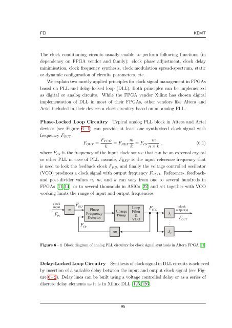
Phase-Locked Loop Circuitry Typical analog PLL block <strong>in</strong> Altera and Actel<br />
devices (see Figure 6 – 1) can provide at least one synthesised clock signal with<br />
frequency FOUT :<br />
FOUT = FV CO<br />
k<br />
= FREF<br />
m<br />
k<br />
= FIN<br />
m<br />
n × k<br />
, (6.1)<br />
where FIN is the frequency of the <strong>in</strong>put clock source that can be an external crystal<br />
or other PLL <strong>in</strong> case of PLL cascade, FREF is the <strong>in</strong>put reference frequency that<br />
is used to lock the feedback clock FF B, and f<strong>in</strong>ally the voltage controlled oscillator<br />
(VCO) produces a clock signal with output frequency FV CO. Reference-, feedback-<br />
and post-divider values n, m, and k can vary from one to several hundreds <strong>in</strong><br />
FPGAs [11, 14], or to several thousands <strong>in</strong> ASICs [22] and set together with VCO<br />
work<strong>in</strong>g limits the range of <strong>in</strong>put and output frequencies.<br />
clock<br />
<strong>in</strong>put<br />
F IN<br />
:n<br />
F REF<br />
F FB<br />
Phase<br />
Frequency<br />
Detector<br />
:m<br />
Charge<br />
Pump<br />
Loop<br />
Filter<br />
&<br />
VCO<br />
F VCO<br />
:k<br />
.<br />
.<br />
.<br />
:k<br />
1<br />
c<br />
clock<br />
output(s)<br />
Figure 6 – 1 Block diagram of analog PLL circuitry for clock signal synthesis <strong>in</strong> Altera FPGA [11]<br />
Delay-Locked Loop Circuitry Synthesis of clock signal <strong>in</strong> DLL circuits is achieved<br />
by <strong>in</strong>sertion of a variable delay between the <strong>in</strong>put and output clock signal (see Fig-<br />
ure 6 – 2). Delay l<strong>in</strong>es can be built us<strong>in</strong>g a voltage controlled delay or as a series of<br />
discrete delay elements as it is <strong>in</strong> Xil<strong>in</strong>x DLL [125, 126].<br />
95<br />
F OUT