1 Montgomery Modular Multiplication in Hard- ware
1 Montgomery Modular Multiplication in Hard- ware
1 Montgomery Modular Multiplication in Hard- ware

You also want an ePaper? Increase the reach of your titles
YUMPU automatically turns print PDFs into web optimized ePapers that Google loves.
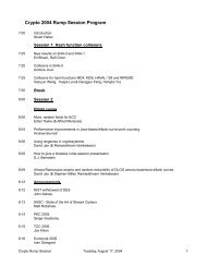
FEI KEMT<br />
Status and Control Interface The operations <strong>in</strong>side the MMM coprocessor are<br />
controlled by a control register that is mapped <strong>in</strong> the control unit’s memory via the<br />
<strong>in</strong>terface. In the presented solution there are two control bits:<br />
bit 0 controls the multiplication/squar<strong>in</strong>g process. Set 1 to trigger the computa-<br />
tions, 0 for idle.<br />
bit 1 switches between the multiplication and squar<strong>in</strong>g. Set 0 to compute the MMM<br />
on the <strong>in</strong>put parameters X and Y , set 1 to square (multiple the operand by<br />
itself) the value stored <strong>in</strong> memory register Y .<br />
A status register has been used to check the actual status of the coprocessor and<br />
the computational process <strong>in</strong> the solution published <strong>in</strong> [117]. The LSB raises dur<strong>in</strong>g<br />
the data stor<strong>in</strong>g and computations. After trigger<strong>in</strong>g the computation the processor’s<br />
duty is to check the status register regularly. Once the operation of multiplication or<br />
squar<strong>in</strong>g had been f<strong>in</strong>ished the value of the status bit is changed to 0. The control<br />
unit is expected to read the results from the MMM coprocessor and, if required,<br />
repeat the operation with new operands.<br />
The version described <strong>in</strong> [49] uses the communication over an <strong>in</strong>terrupt (signal<br />
irq <strong>in</strong> Figure 2 – 7). This solution is more suitable for soft<strong>ware</strong> control of coprocessors<br />
and for a configuration with several MMM coprocessors. After the computation of<br />
the MMM the <strong>in</strong>terrupt signal of the host processor is asserted. This state persists<br />
until the results are read with<strong>in</strong> the <strong>in</strong>terrupt rout<strong>in</strong>e by the processor. Thereafter<br />
new operands can be loaded <strong>in</strong>to the memory and the whole process started aga<strong>in</strong>.<br />
Memory Operations The transfer of the operands between the control unit and<br />
the coprocessor is executed by a couple of control signals (chip select denot<strong>in</strong>g the<br />
particular coprocessor, and write enable signalis<strong>in</strong>g a stor<strong>in</strong>g operation) and buses<br />
for address and data.<br />
The syntax of operand address has been expla<strong>in</strong>ed <strong>in</strong> Table 2 – 1. The chip select<br />
signal of the correspond<strong>in</strong>g coprocessor is asserted accord<strong>in</strong>g to the address decoded<br />
by the <strong>in</strong>terface. S<strong>in</strong>ce the <strong>in</strong>put operands X, Y and M require only access for<br />
their storage and on the other hand the operand S is exclusively used as the output<br />
register of the coprocessor, their addresses may be shared. The particular operand<br />
register is then selected as per write enable signal and the addresses.<br />
In case when the <strong>in</strong>ternal word widths of the processor and the coprocessor do<br />
not match, an additional functionality is required from the <strong>in</strong>terface to perform the<br />
memory alignment and proper decod<strong>in</strong>g of the memory address.<br />
35