1 Montgomery Modular Multiplication in Hard- ware
1 Montgomery Modular Multiplication in Hard- ware
1 Montgomery Modular Multiplication in Hard- ware

You also want an ePaper? Increase the reach of your titles
YUMPU automatically turns print PDFs into web optimized ePapers that Google loves.
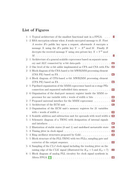
List of Figures<br />
1 – 1 Typical architecture of the smallest functional unit <strong>in</strong> a FPGA. . . . 6<br />
1 – 2 RSA encryption scheme when A sends encrypted message to B. First<br />
A receive B’s public key upon a request, afterwards A encrypts a<br />
message X us<strong>in</strong>g the B’s public key Y = X E mod M. F<strong>in</strong>ally B<br />
decrypts the received message Y us<strong>in</strong>g own private key X = Y D mod<br />
M. . . . . . . . . . . . . . . . . . . . . . . . . . . . . . . . . . . . . . 8<br />
2 – 1 Architecture of a general scalable coprocessor based on separate mem-<br />
ory and ALU connected by w-bit data-path . . . . . . . . . . . . . . 21<br />
2 – 2 One level of the w-bit adder implemented as CPA and CSA with FAs 27<br />
2 – 3 Block diagram of the CSA-based w-bit MWR2MM process<strong>in</strong>g element<br />
(CSA PE) based on FA . . . . . . . . . . . . . . . . . . . . . . . . . . 28<br />
2 – 4 Block diagram of CPA-based w-bit MWR2MM process<strong>in</strong>g element<br />
(CPA PE) based on FA . . . . . . . . . . . . . . . . . . . . . . . . . . 29<br />
2 – 5 Pipel<strong>in</strong>ed organization of the MMM coprocessor based on n-stage PEs<br />
connection and separated embedded data memory . . . . . . . . . . . 30<br />
2 – 6 Organisation of the dual-port memory register <strong>in</strong>side the MMM co-<br />
processor for one variable with e words of width w bits . . . . . . . . 32<br />
2 – 7 Proposed universal <strong>in</strong>terface for the MMM coprocessor . . . . . . . . 34<br />
4 – 1 Architecture of the ECM unit . . . . . . . . . . . . . . . . . . . . . . 58<br />
4 – 2 Organisation of the ECM unit’s memory registers for 21 variables<br />
with e words of width w . . . . . . . . . . . . . . . . . . . . . . . . . 60<br />
4 – 3 Scalable addition and subtraction unit for operands with word width w 63<br />
5 – 1 Schematic diagram of a TRNG with designation of <strong>in</strong>ternal signals<br />
and <strong>in</strong>terfaces . . . . . . . . . . . . . . . . . . . . . . . . . . . . . . . 74<br />
5 – 2 Illustration of stable states (0 and 1) and undef<strong>in</strong>ed metastable state 78<br />
5 – 3 Tim<strong>in</strong>g jitter <strong>in</strong> clock signal . . . . . . . . . . . . . . . . . . . . . . . 81<br />
5 – 4 R<strong>in</strong>g oscillator structures proposed by Golić. . . . . . . . . . . . . . . 83<br />
5 – 5 Block structure of the PLL-TRNG with two PLLs, sampl<strong>in</strong>g gate and<br />
corrector of the output sequence. . . . . . . . . . . . . . . . . . . . . 86<br />
5 – 6 Sampl<strong>in</strong>g of the CLJ clock signal <strong>in</strong>clud<strong>in</strong>g the track<strong>in</strong>g jitter on the<br />
rais<strong>in</strong>g edge of the CLK signal (illustrated for KM = 5 and KD = 7) 86<br />
6 – 1 Block diagram of analog PLL circuitry for clock signal synthesis <strong>in</strong><br />
Altera FPGA [11] . . . . . . . . . . . . . . . . . . . . . . . . . . . . . 95