1 Montgomery Modular Multiplication in Hard- ware
1 Montgomery Modular Multiplication in Hard- ware
1 Montgomery Modular Multiplication in Hard- ware

Create successful ePaper yourself
Turn your PDF publications into a flip-book with our unique Google optimized e-Paper software.
FEI KEMT<br />
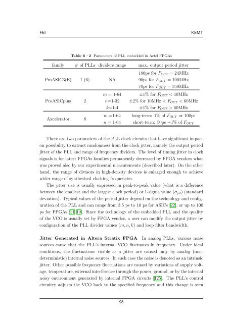
Table 6 – 2 Parameters of PLL embedded <strong>in</strong> Actel FPGAs<br />
family # of PLLs dividers range max. output period jitter<br />
ProASIC3(E) 1 (6) NA<br />
ProASICplus 2<br />
Axcelerator 8<br />
180ps for FOUT = 24MHz<br />
90ps for FOUT = 100MHz<br />
70ps for FOUT = 350MHz<br />
m = 1-64 ±1% for FOUT < 10MHz<br />
n=1-32 ±2% for 10MHz < FOUT < 60MHz<br />
k=1-4 ±1% for FOUT > 60MHz<br />
m =1-64 long-term: 1% of FOUT or 100ps<br />
n = 1-64 short-term: 50ps +1% of FOUT<br />
There are two parameters of the PLL clock circuits that have significant impact<br />
on possibility to extract randomness from the clock jitter, namely the output period<br />
jitter of the PLL and range of frequency dividers. The level of tim<strong>in</strong>g jitter <strong>in</strong> clock<br />
signals is for latest FPGAs families permanently decreased by FPGA vendors what<br />
was proved also by our experimental measurements (described later). On the other<br />
hand, the range of divisors <strong>in</strong> high-density devices is enlarged enough to achieve<br />
wider range of synthesised clock<strong>in</strong>g frequencies.<br />
The jitter size is usually expressed <strong>in</strong> peak-to-peak value (what is a difference<br />
between the smallest and the largest clock period) or 1-sigma value (σjit) (standard<br />
deviation). Typical values of the period jitter depend on the technology and config-<br />
uration of the PLL and can range from 3.5 ps to 10 ps for ASICs [22], or up to 100<br />
ps for FPGAs [11, 19]. S<strong>in</strong>ce the technology of the embedded PLL and the quality<br />
of the VCO is usually set by FPGA vendor, a user can modify the output jitter by<br />
configuration of the PLL divider values (m, n, k) and loop filter bandwidth.<br />
Jitter Generated <strong>in</strong> Altera Stratix FPGA In analog PLLs, various noise<br />
sources cause that the PLL’s <strong>in</strong>ternal VCO fluctuates <strong>in</strong> frequency. Under ideal<br />
conditions, the fluctuations visible as a jitter are caused only by analog (non-<br />
determ<strong>in</strong>istic) <strong>in</strong>ternal noise sources. In such case the noise is denoted as an <strong>in</strong>tr<strong>in</strong>sic<br />
jitter. Other possible frequency fluctuations are caused by variations of supply volt-<br />
age, temperature, external <strong>in</strong>terference through the power, ground, or by the <strong>in</strong>ternal<br />
noisy environment generated by <strong>in</strong>ternal FPGA circuits [125]. The PLL’s control<br />
circuitry adjusts the VCO back to the specified frequency and this change is seen<br />
98