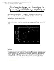
Christoph Haederli - Les thèses en ligne de l'INP - Institut National ...
Christoph Haederli - Les thèses en ligne de l'INP - Institut National ...
Christoph Haederli - Les thèses en ligne de l'INP - Institut National ...

You also want an ePaper? Increase the reach of your titles
YUMPU automatically turns print PDFs into web optimized ePapers that Google loves.
116 NP Control with Carrier based PWM<br />
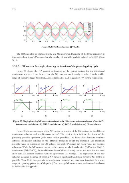
Figure 76, SMC B modulation (α = 0.625)<br />
The SMC can also be operated purely as a MC converter. Balancing of the flying capacitors is<br />
improved, there is no NP curr<strong>en</strong>t, but the number of available levels is reduced to N/2+1 (from<br />
N+1).<br />
5.3.2.3 NP curr<strong>en</strong>t for single phase leg in function of the phase leg duty cycle<br />
Figure 77 shows the NP curr<strong>en</strong>t in function of the output voltage for the introduced<br />
modulation schemes. It can be se<strong>en</strong> that the NP curr<strong>en</strong>t can effectively be reduced in the middle<br />
range of output voltages. Note that s avg is used instead of α L. See equation (40) for the relationship.<br />
1<br />
α2<br />
α1<br />
0<br />
-1 0 1<br />
s avg<br />
1<br />
α2<br />
α1<br />
0<br />
-1 0 1<br />
s avg<br />
1<br />
α2<br />
α1<br />
0<br />
-1 0 1<br />
s avg<br />
1<br />
α2 α1<br />
0<br />
-1 0 1<br />
s avg<br />
1<br />
I NP / I out<br />
1<br />
I NP / I out<br />
1<br />
I NP / I out<br />
1<br />
I NP / I out<br />
0<br />
-1 0 1<br />
s avg<br />
0<br />
-1 0 1<br />
s avg<br />
0<br />
-1 0 1<br />
s avg<br />
0<br />
-1 0 1<br />
s avg<br />
(a) (b) (c) (d)<br />
Figure 77, Single phase leg NP curr<strong>en</strong>t functions for the differ<strong>en</strong>t modulation schemes of the SMC:<br />
(a) standard modulation, (b) SMC A modulation, (c) SMC B modulation, (d) FC modulation<br />
Figure 78 shows an example of the NP curr<strong>en</strong>t in function of the CM voltage for the differ<strong>en</strong>t<br />
modulation schemes and combinations thereof. The vertical lines indicate the limits of the<br />
physically possible operation (only inner section possible). The lower four functions combine<br />
differ<strong>en</strong>t modulation schemes in the differ<strong>en</strong>t phases to obtain the minimum and maximum<br />
possible values in function of the CM voltage; the total NP curr<strong>en</strong>t can reach values not possible<br />
otherwise. While the NP curr<strong>en</strong>t cannot reach zero for standard modulation (INP-std) or SMC A<br />
modulation (INP-SMCA), the combination thereof (I-std+A-max) crosses the zero line and does<br />
allow zero NP curr<strong>en</strong>t operation with the appropriate CM voltage. The application of the new<br />
schemes increases the range of possible NP curr<strong>en</strong>ts significantly and more powerful NP control is<br />
possible. Table 85 in the app<strong>en</strong>dix shows absolute minimum and maximum functions for a wi<strong>de</strong><br />
range of operating points (any CM applied).Zero average NP curr<strong>en</strong>t areas are increased as shown<br />
in Table 86 in the app<strong>en</strong>dix.