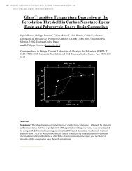
Christoph Haederli - Les thèses en ligne de l'INP - Institut National ...
Christoph Haederli - Les thèses en ligne de l'INP - Institut National ...
Christoph Haederli - Les thèses en ligne de l'INP - Institut National ...

Create successful ePaper yourself
Turn your PDF publications into a flip-book with our unique Google optimized e-Paper software.
3-L DC Link ML Converter Properties 63<br />
1. Standard PD PWM or SVM with new CM injection concepts and subsequ<strong>en</strong>t state<br />
optimization for capacitor control for medium and high switching frequ<strong>en</strong>cies (chapter 4<br />
and paragraph 6.1)<br />
2. Optimal sequ<strong>en</strong>ce SVM, with only 3 vectors to be applied per modulation period,<br />
applicable to low switching frequ<strong>en</strong>cy applications (paragraph 6.2)<br />
4.4.6 Modulator implem<strong>en</strong>tation and experim<strong>en</strong>tal verification<br />
Differ<strong>en</strong>t modulator implem<strong>en</strong>tations have be<strong>en</strong> used in the frame of this thesis. The<br />
modulator for the experim<strong>en</strong>tal verification of the SMC schemes (5.3.4) has be<strong>en</strong> implem<strong>en</strong>ted<br />
totally on an FPGA with a g<strong>en</strong>eric PD PWM modulator and a subsequ<strong>en</strong>t state machine choosing<br />
the appropriate converter states (Figure 53). This modulator runs on a DSP based control system<br />
by LAPLACE [66]. The optimal sequ<strong>en</strong>ce modulator introduced in 6.2 runs on an industrial control<br />
system (AC 800PEC by ABB). The co<strong>de</strong> is implem<strong>en</strong>ted in MATLAB/Simulink. OPCoDe<br />
(Optimized Process of Co<strong>de</strong> Developm<strong>en</strong>t) g<strong>en</strong>erates the runtime co<strong>de</strong> automatically from the<br />
Simulink and Matlab files.<br />
Figure 54, ABB’s AC 800PEC, core of the OPCoDe system<br />
A third separate modulator is running on the same OPCoDe system, is implem<strong>en</strong>ted also in<br />
Matlab but inclu<strong>de</strong>s multiple modulators: all CB PWM schemes according to the paragraphs 5.1<br />
and 5, as well as the SVM scheme with virtual vectors introduced in paragraph 6.1. These schemes<br />
are seamlessly integrated and can changeover from one to the other scheme in operation anytime.<br />
This feature is required by the hysteresis controller proposed in paragraph 7.3. The CB part of the<br />
modulator has asymmetric sampling, PD double edge modulation. Differ<strong>en</strong>t PD PWM schemes<br />
(e.g. 3 rd harmonic injection or CSPD PWM) can be chos<strong>en</strong>. Switching times are pre-calculated<br />
(rather than <strong>de</strong>termined by an actual refer<strong>en</strong>ce carrier comparison) and communicated to the<br />
FPGA for gate signal g<strong>en</strong>eration. In this way, the gate signal g<strong>en</strong>eration on the FPGA can easily be<br />
shared with the SVM schemes, which are based on the NTV method. A calculation method with<br />
non perp<strong>en</strong>dicular coordinates similar to [34], [67] or [68] is used for fast calculation. The same<br />
implem<strong>en</strong>tation of the modulator (same m-file) is used for simulation and experim<strong>en</strong>tal verification,<br />
which <strong>en</strong>sures good correspond<strong>en</strong>ce betwe<strong>en</strong> simulation and real operation of the converter.<br />
A low power 5-L ANPC prototype (6kVA) has be<strong>en</strong> used for all experim<strong>en</strong>tal verification<br />
regarding ANPC. The prototype has be<strong>en</strong> specified for control investigations (rather than high<br />
power d<strong>en</strong>sity) providing easy access to all relevant signals and flexible configuration of DC link<br />
and flying capacitors.