Christoph Haederli - Les thèses en ligne de l'INP - Institut National ...
Christoph Haederli - Les thèses en ligne de l'INP - Institut National ...
Christoph Haederli - Les thèses en ligne de l'INP - Institut National ...

You also want an ePaper? Increase the reach of your titles
YUMPU automatically turns print PDFs into web optimized ePapers that Google loves.
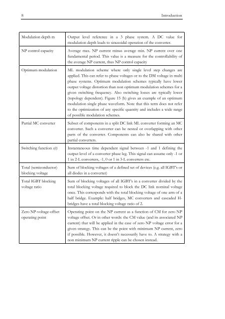
8 Introduction<br />
Modulation <strong>de</strong>pth m<br />
NP control capacity<br />
Optimum modulation<br />
Partial MC converter<br />
Switching function s(t)<br />
Total (semiconductor)<br />
blocking voltage<br />
Total IGBT blocking<br />
voltage ratio<br />
Zero NP-voltage-offset<br />
operating point<br />
Output level refer<strong>en</strong>ce in a 3 phase system. A DC value for<br />
modulation <strong>de</strong>pth leads to sinusoidal operation of the converter.<br />
Average max. NP curr<strong>en</strong>t minus average min. NP curr<strong>en</strong>t over one<br />
fundam<strong>en</strong>tal period. This value is a measure for the controllability of<br />
the average NP curr<strong>en</strong>t, thus NP control capacity<br />
ML modulation scheme where only single level step changes are<br />
applied. This can refer to phase voltages or to the DM voltage in multi<br />
phase systems. Optimum modulation schemes typically have lower<br />
output voltage distortion than non optimum modulation schemes for a<br />
giv<strong>en</strong> switching frequ<strong>en</strong>cy. Also switching losses are typically lower<br />
(topology <strong>de</strong>p<strong>en</strong>d<strong>en</strong>t). Figure 15 (b) gives an example of an optimum<br />
modulation single phase waveform. Note that this term does not refer<br />
to the optimization of any specific quantity and inclu<strong>de</strong>s a wi<strong>de</strong> range<br />
of possible modulation schemes.<br />
Subset of compon<strong>en</strong>ts in a split DC link ML converter forming an MC<br />
converter. Such a converter can be nested or overlapping with other<br />
parts of the converter. Compon<strong>en</strong>ts can also be shared with other<br />
partial converters.<br />
Instantaneous time <strong>de</strong>p<strong>en</strong>dant signal betwe<strong>en</strong> -1 and 1 <strong>de</strong>fining the<br />
output level of a converter phase leg. This signal can assume only -1 or<br />
1 in 2-L converters, -1, 0 or 1 in 3-L converters etc.<br />
Sum of blocking voltages of a <strong>de</strong>fined set of <strong>de</strong>vices (e.g. all IGBT’s or<br />
all dio<strong>de</strong>s in a converter)<br />
Sum of blocking voltages of all IGBT’s in a converter divi<strong>de</strong>d by the<br />
total blocking voltage required to block the DC link nominal voltage<br />
once. This corresponds with the total blocking voltage of one arm of a<br />
half bridge. Example: half bridges, MC converters and casca<strong>de</strong>d H-<br />
bridges have a total blocking voltage ratio of 2.<br />
Operating point on the NP curr<strong>en</strong>t as a function of CM for zero NP<br />
voltage offset. Or in other words: the CM value (and its associated NP<br />
curr<strong>en</strong>t) that will be applied in the case of zero NP voltage error for a<br />
giv<strong>en</strong> strategy. This can be the point with minimum NP curr<strong>en</strong>t, zero<br />
if possible. However, it doesn’t necessarily have to. A strategy with a<br />
non minimum NP curr<strong>en</strong>t ripple can be chos<strong>en</strong> instead.