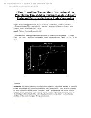
Christoph Haederli - Les thèses en ligne de l'INP - Institut National ...
Christoph Haederli - Les thèses en ligne de l'INP - Institut National ...
Christoph Haederli - Les thèses en ligne de l'INP - Institut National ...

Create successful ePaper yourself
Turn your PDF publications into a flip-book with our unique Google optimized e-Paper software.
142 NP Control with Optimal Sequ<strong>en</strong>ce SVM<br />
TABLE 56, PROPERTIES OF SCHEME ALLOWING MULTIPLE COMMUTATIONS<br />
1. Discontinuous modulation (only 2 phases operating) is possible<br />
2. Decoupling of CM from sequ<strong>en</strong>ce ori<strong>en</strong>tation<br />
3. Loss balancing betwe<strong>en</strong> differ<strong>en</strong>t phases<br />
4. Higher common mo<strong>de</strong> jump within one modulation cycle to improve NP control<br />
5. The switching losses do not necessarily increase with double commutations. If the two phases<br />
with the lower curr<strong>en</strong>ts are switched, the third curr<strong>en</strong>t is the sum of the two lower curr<strong>en</strong>ts<br />
and the resulting switching losses also roughly add up to the value of a single commutation of<br />
the highest curr<strong>en</strong>t.<br />
6. The complexity and calculation effort is significantly increased. Double commutations allow<br />
for up to 6 redundant states in each step of a sequ<strong>en</strong>ce. As a result one individual tree of<br />
sequ<strong>en</strong>ces may have 6^3 = 216 possible sequ<strong>en</strong>ces. Also the maximum number of starting<br />
states is increased, so that significantly more than 1000 sequ<strong>en</strong>ces are possible in the worst<br />
case (for the ANPC 1).<br />
6.2.1.3 Definition of the objective function<br />
The DM output voltage is a constraint which is satisfied by the nearest three vectors<br />
modulation. All consi<strong>de</strong>red sequ<strong>en</strong>ces th<strong>en</strong> result in the correct output voltage. Therefore, no<br />
converter output quantity needs to be integrated in the objective function. NP and FC voltages as<br />
well as losses can be predicted based on the converter mo<strong>de</strong>l and the sequ<strong>en</strong>ces of states<br />
<strong>de</strong>termined.<br />
TABLE 57, QUANTITIES TO BE USED IN OBJECTIVE FUNCTION<br />
Quantity to be integrated in objective<br />
function<br />
Switching losses<br />
Voltage <strong>de</strong>viation in flying capacitors<br />
Voltage <strong>de</strong>viation in NP<br />
Output quantity THD or WTHD<br />
CM voltage optimization<br />
Appar<strong>en</strong>t output switching frequ<strong>en</strong>cy<br />
Comm<strong>en</strong>t<br />
The switching loss cost is primarily proportional to the total<br />
losses, but can also inclu<strong>de</strong> a term on loss distribution<br />
Square function to minimize total <strong>en</strong>ergy in flying capacitors<br />
or piecewise linear function to achieve quasi tolerance band<br />
behavior<br />
Square function to minimize total <strong>en</strong>ergy in NP or piecewise<br />
linear function to achieve quasi tolerance band behavior<br />
Approximation algorithms based on the output voltage can<br />
be used (e.g. harmonic flux trajectory, [107]) or load mo<strong>de</strong>ls<br />
can be used to <strong>de</strong>termine curr<strong>en</strong>t or torque ripple.<br />
CM voltage is relevant in motor applications because of the<br />
bearing curr<strong>en</strong>t g<strong>en</strong>eration and isolation stress.<br />
A certain appar<strong>en</strong>t output switching frequ<strong>en</strong>cy may be<br />
required to optimally operate a filter or to avoid certain<br />
frequ<strong>en</strong>cies (mechanical resonances, signaling)