

Soft-Core Processor Design - CiteSeer
Soft-Core Processor Design - CiteSeer
Soft-Core Processor Design - CiteSeer

You also want an ePaper? Increase the reach of your titles
YUMPU automatically turns print PDFs into web optimized ePapers that Google loves.
uilt using techniques proven to be appropriate for ASIC processors. However, having in mind<br />
the differences in the implementation technologies, it is not obvious if the same rules that hold for<br />
ASIC designs can be applied to designs for FPGAs. This work differs from previous work in that<br />
it tries to give an insight into the development process, including the design choices and trade-<br />
offs in developing a soft-core processor. Since the design cycles in the FPGA design<br />
methodology are much shorter than for ASICs, it is practical to improve the design incrementally,<br />
using feedback from the previous steps. Many decisions in this work were guided by such<br />
feedback, not by the traditional wisdom. The result is an architecture, significantly different than<br />
the Altera Nios, with an average performance very close to the original processor. Although the<br />
FPGA design flow reduces the time needed to explore the design space, the design space is still<br />
vast, so this work can serve as a basis for future research.<br />
2.2. FPGA technology<br />
FPGA devices are programmable to implement arbitrary user logic. To support this<br />
programmability, FPGA devices contain three types of resources: logic blocks, I/O blocks, and<br />
programmable interconnection.<br />
Most FPGAs contain logic blocks that consist of a lookup table (LUT), and a flip-flop. A LUT<br />
can be programmed to implement any logic function of its inputs. A LUT with n inputs is called<br />
an n-LUT. An n-LUT is internally implemented as a set of 2-to-1 multiplexers, functioning as a<br />
2 n -to-1 multiplexer. Multiplexer inputs are programmable, while select lines are used for inputs of<br />
the implemented function. Research has shown that 4-LUTs are an optimal choice for<br />
FPGAs [11].<br />
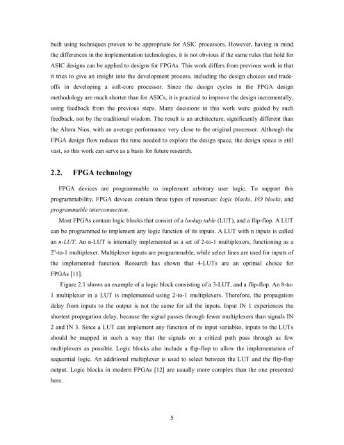
Figure 2.1 shows an example of a logic block consisting of a 3-LUT, and a flip-flop. An 8-to-<br />
1 multiplexer in a LUT is implemented using 2-to-1 multiplexers. Therefore, the propagation<br />
delay from inputs to the output is not the same for all the inputs. Input IN 1 experiences the<br />
shortest propagation delay, because the signal passes through fewer multiplexers than signals IN<br />
2 and IN 3. Since a LUT can implement any function of its input variables, inputs to the LUTs<br />
should be mapped in such a way that the signals on a critical path pass through as few<br />
multiplexers as possible. Logic blocks also include a flip-flop to allow the implementation of<br />
sequential logic. An additional multiplexer is used to select between the LUT and the flip-flop<br />
output. Logic blocks in modern FPGAs [12] are usually more complex than the one presented<br />
here.<br />
5


