

Soft-Core Processor Design - CiteSeer
Soft-Core Processor Design - CiteSeer
Soft-Core Processor Design - CiteSeer

Create successful ePaper yourself
Turn your PDF publications into a flip-book with our unique Google optimized e-Paper software.
parameters include the general-purpose register file size, the choice to implement the instruction<br />
decoder in on-chip memory or in logic, the size of the FIFO buffer in the processor’s prefetch<br />
unit, and the starting and vector table memory addresses.<br />
The UT Nios can be used directly in any system generated by the SOPC builder. If the system<br />
contains the 32-bit Altera Nios, the module implementing the Altera Nios can be replaced by the<br />
module implementing the UT Nios. This can be done by simply replacing the Verilog file that<br />
implements the Altera Nios. After setting the UT Nios parameters according to the system<br />
requirements, the system can be compiled in Quartus II and downloaded to an FPGA.<br />
The UT Nios consists of two main modules; datapath and control unit. The processor datapath<br />
defines interconnections between the processor modules and defines how data propagates<br />
between the pipeline stages. The control unit is a finite state machine that produces the control<br />
signals for modules in the datapath. In the sections that follow we present high-level<br />
implementation details of the UT Nios. For the low-level details, the UT Nios Verilog code<br />
should be consulted.<br />
4.1. UT Nios Datapath<br />
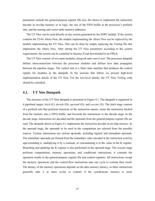
The structure of the UT Nios datapath is presented in Figure 4.1. The datapath is organized in<br />
4 pipelined stages: fetch (F), decode (D), operand (O), and execute (X). The fetch stage consists<br />
of a prefetch unit that performs functions of the instruction master, stores the instruction fetched<br />
from the memory into a FIFO buffer, and forwards the instructions to the decode stage. In the<br />
decode stage, instructions are decoded and the operands from the general-purpose register file are<br />
read. The datapath shown in Figure 4.1 implements the instruction decoder in on-chip memory. In<br />
the operand stage, the operands to be used in the computation are selected from the possible<br />
sources. Various instructions use various operands, including register and immediate operands.<br />
The immediate operands are formed from the immediate value encoded in the instruction word by<br />
sign-extending it, multiplying it by a constant, or concatenating it to the value in the K register.<br />
Branching and updating the K register is also performed in the operand stage. The execute stage<br />
performs computations, memory operations, and conditional instructions; it commits the<br />
operation results to the general-purpose register file and control registers. All instructions except<br />
the memory operations and the control-flow instructions take one cycle to commit their result.<br />
The latency of the memory operations depends on the data memory latency, so these instructions<br />
generally take 2 or more cycles to commit if the synchronous memory is used.<br />
31


