

Soft-Core Processor Design - CiteSeer
Soft-Core Processor Design - CiteSeer
Soft-Core Processor Design - CiteSeer

Create successful ePaper yourself
Turn your PDF publications into a flip-book with our unique Google optimized e-Paper software.
� ��¥<br />
� ���<br />
� ���<br />
¢¤£¦¥<br />
¢¤£¦¥<br />
¢¤£¦¥<br />
¢¤£¦¥<br />
¢¤£¦¥<br />
¢¤£¦¥<br />
¢¤£¦¥<br />
¢¤£¦¥<br />
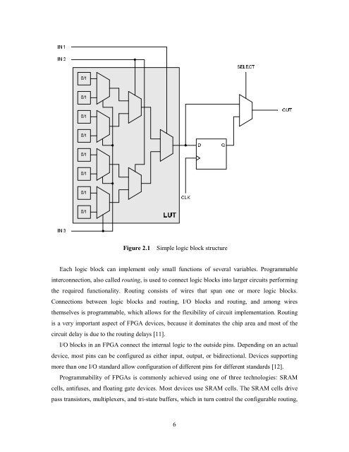
Each logic block can implement only small functions of several variables. Programmable<br />
interconnection, also called routing, is used to connect logic blocks into larger circuits performing<br />
the required functionality. Routing consists of wires that span one or more logic blocks.<br />
Connections between logic blocks and routing, I/O blocks and routing, and among wires<br />
themselves is programmable, which allows for the flexibility of circuit implementation. Routing<br />
is a very important aspect of FPGA devices, because it dominates the chip area and most of the<br />
circuit delay is due to the routing delays [11].<br />
�����<br />
I/O blocks in an FPGA connect the internal logic to the outside pins. Depending on an actual<br />
device, most pins can be configured as either input, output, or bidirectional. Devices supporting<br />
more than one I/O standard allow configuration of different pins for different standards [12].<br />
Programmability of FPGAs is commonly achieved using one of three technologies: SRAM<br />
cells, antifuses, and floating gate devices. Most devices use SRAM cells. The SRAM cells drive<br />
pass transistors, multiplexers, and tri-state buffers, which in turn control the configurable routing,<br />
6<br />
�����<br />
Figure 2.1 Simple logic block structure<br />
¡<br />
�����������<br />
§©¨��


