- Page 3:
DEVELOPMENTS IN CERAMIC MATERIALS R
- Page 6 and 7:
Copyright © 2007 by Nova Science P
- Page 9 and 10:
PREFACE Ceramics are refractory, in
- Page 11 and 12:
Preface ix crystals is discussed. A
- Page 13:
Preface xi spectra and the directio
- Page 16 and 17:
2 Leslie G. Cecil comprehensive dat
- Page 18 and 19:
4 Leslie G. Cecil Ringle et al. (19
- Page 20 and 21:
6 Leslie G. Cecil The main architec
- Page 22 and 23:
8 Leslie G. Cecil can study “the
- Page 24 and 25:
10 Leslie G. Cecil Middleton et al.
- Page 26 and 27:
12 Leslie G. Cecil The laser ablate
- Page 28 and 29:
14 Leslie G. Cecil There are two ge
- Page 30 and 31:
16 Leslie G. Cecil distinct recipes
- Page 32 and 33:
18 Leslie G. Cecil second group (Fi
- Page 34 and 35:
20 Leslie G. Cecil The Vitzil-Orang
- Page 36 and 37:
22 Leslie G. Cecil Table 3. Mahalan
- Page 38 and 39:
24 Leslie G. Cecil Ixlú and Ch’i
- Page 40 and 41:
26 Leslie G. Cecil structures (D. R
- Page 42 and 43:
28 Leslie G. Cecil paste and Macanc
- Page 44 and 45:
30 Leslie G. Cecil Bieber, A. M. Jr
- Page 46 and 47:
32 Leslie G. Cecil Kepecs, S. M., a
- Page 48 and 49:
34 Leslie G. Cecil Schele, L., Grub
- Page 50 and 51:
36 Z. C. Li, Z. J. Pei and C. Tread
- Page 52 and 53:
38 Z. C. Li, Z. J. Pei and C. Tread
- Page 54 and 55:
40 Z. C. Li, Z. J. Pei and C. Tread
- Page 56 and 57:
42 Z. C. Li, Z. J. Pei and C. Tread
- Page 58 and 59:
44 Z. C. Li, Z. J. Pei and C. Tread
- Page 60 and 61:
46 Z. C. Li, Z. J. Pei and C. Tread
- Page 62 and 63:
48 Z. C. Li, Z. J. Pei and C. Tread
- Page 64 and 65:
50 Z. C. Li, Z. J. Pei and C. Tread
- Page 66 and 67:
52 Z. C. Li, Z. J. Pei and C. Tread
- Page 68 and 69:
54 T. T. Basiev, V. A. Demidenko, K
- Page 70 and 71:
56 T. T. Basiev, V. A. Demidenko, K
- Page 72 and 73:
58 T. T. Basiev, V. A. Demidenko, K
- Page 74 and 75:
60 T. T. Basiev, V. A. Demidenko, K
- Page 76 and 77:
62 I, % 100 80 60 40 20 0 T. T. Bas
- Page 78 and 79:
64 T. T. Basiev, V. A. Demidenko, K
- Page 80 and 81:
66 T. T. Basiev, V. A. Demidenko, K
- Page 82 and 83:
68 Fluorescence, a.u. 1 T. T. Basie
- Page 84 and 85:
70 Fluorescence, a.u. 1 0.1 0.01 0.
- Page 86 and 87:
72 T. T. Basiev, V. A. Demidenko, K
- Page 88 and 89:
74 T. T. Basiev, V. A. Demidenko, K
- Page 90 and 91:
76 T. T. Basiev, V. A. Demidenko, K
- Page 92 and 93:
78 k, cm -1 20 18 16 14 12 10 8 6 4
- Page 94 and 95:
80 T. T. Basiev, V. A. Demidenko, K
- Page 96 and 97:
82 Photon counts 300 250 200 150 10
- Page 98 and 99:
84 Fluorescence, a.u. I transfer ,
- Page 100 and 101:
86 ln(I transfer (t)) -4.2 -4.4 -4.
- Page 102 and 103:
88 Fluorescence, a.u. I transfer ,
- Page 104 and 105:
90 T. T. Basiev, V. A. Demidenko, K
- Page 106 and 107:
92 T. T. Basiev, V. A. Demidenko, K
- Page 108 and 109:
94 T. T. Basiev, V. A. Demidenko, K
- Page 111 and 112:
In: Developments in Ceramic Materia
- Page 113 and 114:
Synthesis, Spectroscopic and Magnet
- Page 115 and 116:
a c Synthesis, Spectroscopic and Ma
- Page 117 and 118:
Synthesis, Spectroscopic and Magnet
- Page 119 and 120:
Transmission Transmission Transmiss
- Page 121 and 122:
Synthesis, Spectroscopic and Magnet
- Page 123 and 124:
Synthesis, Spectroscopic and Magnet
- Page 125 and 126:
Synthesis, Spectroscopic and Magnet
- Page 127 and 128:
Synthesis, Spectroscopic and Magnet
- Page 129 and 130:
Synthesis, Spectroscopic and Magnet
- Page 131 and 132:
Synthesis, Spectroscopic and Magnet
- Page 133 and 134:
Synthesis, Spectroscopic and Magnet
- Page 135 and 136:
Synthesis, Spectroscopic and Magnet
- Page 137 and 138:
Sm (J/Kmol) Sm (J/Kmol) 15 10 5 Syn
- Page 139 and 140:
Synthesis, Spectroscopic and Magnet
- Page 141 and 142:
Synthesis, Spectroscopic and Magnet
- Page 143 and 144:
Synthesis, Spectroscopic and Magnet
- Page 145 and 146:
Intensity (a.u.) Intensity (a.u.) 8
- Page 147 and 148:
Synthesis, Spectroscopic and Magnet
- Page 149 and 150:
Synthesis, Spectroscopic and Magnet
- Page 151 and 152:
Synthesis, Spectroscopic and Magnet
- Page 153 and 154:
Synthesis, Spectroscopic and Magnet
- Page 155 and 156:
In: Developments in Ceramic Materia
- Page 157 and 158:
The Use of Ceramic Pots in Old Wors
- Page 159 and 160:
The Use of Ceramic Pots in Old Wors
- Page 161 and 162:
The Use of Ceramic Pots in Old Wors
- Page 163 and 164:
3.2. Wall-in Positions The Use of C
- Page 165 and 166:
The Use of Ceramic Pots in Old Wors
- Page 167 and 168:
The Use of Ceramic Pots in Old Wors
- Page 169 and 170:
The Use of Ceramic Pots in Old Wors
- Page 171 and 172:
IACC ( τ ) = t2 ∫ The Use of Cer
- Page 173 and 174:
The Use of Ceramic Pots in Old Wors
- Page 175 and 176:
where σ res is the scattering cros
- Page 177 and 178:
The Use of Ceramic Pots in Old Wors
- Page 179 and 180:
D50 0.8 0.7 0.6 0.5 0.4 0.3 The Use
- Page 181 and 182:
Definition (D50) 1 0.95 0.9 0.85 0.
- Page 183 and 184:
The Use of Ceramic Pots in Old Wors
- Page 185 and 186:
The Use of Ceramic Pots in Old Wors
- Page 187 and 188:
In: Developments in Ceramic Materia
- Page 189 and 190:
Modeling of Thermal Transport in Ce
- Page 191 and 192:
Modeling of Thermal Transport in Ce
- Page 193 and 194:
Modeling of Thermal Transport in Ce
- Page 195 and 196:
Modeling of Thermal Transport in Ce
- Page 197 and 198:
Modeling of Thermal Transport in Ce
- Page 199 and 200:
Modeling of Thermal Transport in Ce
- Page 201 and 202:
Modeling of Thermal Transport in Ce
- Page 203 and 204:
Modeling of Thermal Transport in Ce
- Page 205 and 206:
q x = Modeling of Thermal Transport
- Page 207 and 208:
Modeling of Thermal Transport in Ce
- Page 209 and 210:
Modeling of Thermal Transport in Ce
- Page 211 and 212: Modeling of Thermal Transport in Ce
- Page 213 and 214: Modeling of Thermal Transport in Ce
- Page 215 and 216: Modeling of Thermal Transport in Ce
- Page 217 and 218: Modeling of Thermal Transport in Ce
- Page 219 and 220: Modeling of Thermal Transport in Ce
- Page 221 and 222: Modeling of Thermal Transport in Ce
- Page 223: Modeling of Thermal Transport in Ce
- Page 226 and 227: 212 R. Ramesh, H. Kara, Ron Stevens
- Page 228 and 229: 214 R. Ramesh, H. Kara, Ron Stevens
- Page 230 and 231: 216 R. Ramesh, H. Kara, Ron Stevens
- Page 232 and 233: 218 R. Ramesh, H. Kara, Ron Stevens
- Page 234 and 235: 220 ε S 33 R. Ramesh, H. Kara, Ron
- Page 236 and 237: 222 R. Ramesh, H. Kara, Ron Stevens
- Page 238 and 239: 224 R. Ramesh, H. Kara, Ron Stevens
- Page 240 and 241: 226 R. Ramesh, H. Kara, Ron Stevens
- Page 242 and 243: 228 R. Ramesh, H. Kara, Ron Stevens
- Page 244 and 245: 230 R. Ramesh, H. Kara, Ron Stevens
- Page 246 and 247: 232 R. Ramesh, H. Kara, Ron Stevens
- Page 248 and 249: 234 R. Ramesh, H. Kara, Ron Stevens
- Page 250 and 251: 236 R. Ramesh, H. Kara, Ron Stevens
- Page 252 and 253: 238 R. Ramesh, H. Kara, Ron Stevens
- Page 254 and 255: 240 R. Ramesh, H. Kara, Ron Stevens
- Page 256 and 257: 242 Development of Display Technolo
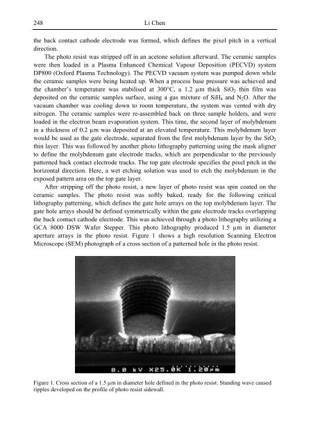
- Page 258 and 259: 244 Li Chen technology moved to the
- Page 260 and 261: 246 Li Chen The continuing evolutio
- Page 264 and 265: 250 Li Chen Figure 3. Vertical side
- Page 266 and 267: 252 Li Chen Figure 6. Molybdenum mi
- Page 268 and 269: 254 Li Chen Figure 8(a). I-V curve
- Page 270 and 271: 256 Li Chen Figure 9. Life time tes
- Page 272 and 273: 258 Figure 11(a). Plasma generated
- Page 274 and 275: 260 Li Chen [13] C.A. Spindt, K.R.
- Page 276 and 277: 262 S. Ardizzone, C. L. Bianchi, G.
- Page 278 and 279: 264 S. Ardizzone, C. L. Bianchi, G.
- Page 280 and 281: 266 S. Ardizzone, C. L. Bianchi, G.
- Page 282 and 283: 268 S. Ardizzone, C. L. Bianchi, G.
- Page 284 and 285: 270 S. Ardizzone, C. L. Bianchi, G.
- Page 286 and 287: 272 S. Ardizzone, C. L. Bianchi, G.
- Page 288 and 289: 274 S. Ardizzone, C. L. Bianchi, G.
- Page 290 and 291: 276 S. Ardizzone, C. L. Bianchi, G.
- Page 292 and 293: 278 S. Ardizzone, C. L. Bianchi, G.
- Page 295 and 296: A absorption spectra, 66, 67, 77, 7
- Page 297 and 298: correlation function, 156 corrosion
- Page 299 and 300: group membership, 13, 20, 21, 22, 2
- Page 301 and 302: microstructure(s), x, xi, 73, 74, 2
- Page 303 and 304: efraction index, 61 refractive inde
- Page 305 and 306: time, vii, ix, 1, 3, 7, 8, 11, 26,