Doktorarbeit_Mairoser.pdf - OPUS - Universität Augsburg
Doktorarbeit_Mairoser.pdf - OPUS - Universität Augsburg
Doktorarbeit_Mairoser.pdf - OPUS - Universität Augsburg

Sie wollen auch ein ePaper? Erhöhen Sie die Reichweite Ihrer Titel.
YUMPU macht aus Druck-PDFs automatisch weboptimierte ePaper, die Google liebt.
A. Ergänzungen zur Dünnfilmtechnologie<br />
ew articles | insight<br />
NAture mAterIAls doi: 10.1038/nmat2380<br />
0<br />
–1<br />
Stuttgart<br />
(1.2 MV)<br />
Dietrich<br />
(200 kV)<br />
Aberration-corrected<br />
electron microscope<br />
TEAM/<br />
CREST<br />
NION<br />
Haider<br />
(200 kV)<br />
10 0<br />
10 1<br />
Source<br />
2<br />
3<br />
4<br />
Light<br />
microscope<br />
Electron microscope<br />
Zach, Haider<br />
(1 kV SEM)<br />
Borries and Ruska<br />
Marton, Ardenne<br />
(100 kV)<br />
Amici<br />
Abbe<br />
Ruska (75 kV)<br />
10 2<br />
10 3<br />
10 4<br />
Feature size (Å)<br />
Lenses<br />
5<br />
800<br />
Ross<br />
1850 1900<br />
1950 2000 2050<br />
Year<br />
Sample<br />
ardware advances in imaging microscopies. Optical<br />
y reached its far-field diffraction limit roughly a century ago.<br />
icroscopy, exploiting the reduction in electron wavelength with<br />
beam voltage, showed steady increases in resolving power for<br />
ars, until limited by radiation damage. Recent developments<br />
g electron-optical aberrations have led to improvements in<br />
ower without having to increase the electron beam energy.<br />
till far from their ultimate diffraction limits, corrected electron<br />
es have already demonstrated the ability to resolve submage<br />
features. (Adapted from ref. 114; © 2009 Elsevier.)<br />
ADF<br />
detector<br />
projections increases roughly as the square of the resoluen<br />
improvements in resolution by a factor of two or three<br />
ke a dramatic difference. Even when such small distances<br />
ed to be measured, a smaller probe size allows for higher<br />
mages and improved detectability of single dopant atoms,<br />
studies of a wider range of dopant species and thicker,<br />
istic, substrates.<br />
rticle will explore the limits and opportunities for the<br />
ration of aberration-corrected microscopes. After a brief<br />
n of the STEM itself, the improvements in resolution and<br />
ue to aberration-corrected optics and improved electron<br />
re detailed. Improved energy resolution from monors<br />
and higher-resolution spectrometers has enabled nanosurements<br />
of the photonic properties of materials and<br />
es. Finally, with the improvements in instrumentation, it<br />
ple itself and the radiation dose it can tolerate that seems<br />
the limit to signal and resolution.<br />
ning transmission electron microscope<br />
TEM to include the necessary field-emission source and<br />
um needed to keep samples clean during irradiation was<br />
by Crewe in 1964 (ref. 35), and within a few years they<br />
onstrating images of single heavy atoms 15 and their difoss<br />
thin carbon films 36 . The popular dark-field and high-<br />
-field imaging modes were demonstrated early during the<br />
development, including in the collection of lattice images<br />
oparticles 37 . As the original microscopes were intended for<br />
research, these samples were used more as resolution tests<br />
materials studies — with one exception being the study<br />
t particles 19 . Adoption of the STEM technique was slow<br />
difficulties in sample preparation 190of<br />
bulk materials and a<br />
despread instrument availability as a result of the vacuum<br />
onics requirements.<br />
Electron<br />
spectrometer<br />
© 2009 Macmillan Publishers Limited. All rights reserved<br />
Figure 3 | major elements of a scanning transmission electron<br />
microscope. A high-brightness electron source produces a 100–300- keV<br />
electron beam with an energy spread of 0.3–1 eV, which can be narrowed<br />
to below 100 meV with a monochromator. Round magnetic lenses and<br />
corrective multipole optics focus the beam to a spot size of between<br />
0.05 and ~0.3 nm, which is scanned across an electron-transparent sample.<br />
To a first approximation, when the beam is placed on an atom column,<br />
strong Rutherford-like scattering deflects the transmitted electrons to form<br />
brighter features in an annular dark-field (ADF) image, with less scattering<br />
between the columns. Inelastic scattering is strongly peaked in the forward<br />
direction and is collected simultaneously with the ADF signal. The energy<br />
losses of the transmitted electrons reflect characteristic excitations of<br />
the sample in a frequency range spanning the near-infrared to hard X-ray<br />
regions, allowing electronic and elemental identification from a single<br />
column of atoms.<br />
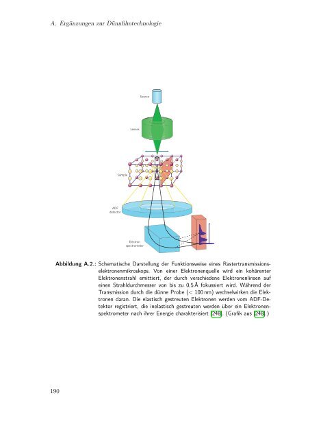
Abbildung A.2.: Schematische Darstellung der Funktionsweise eines Rastertransmissionselektronenmikroskops.<br />
Von einer Elektronenquelle wird ein kohärenter<br />
Elektronenstrahl emittiert, der durch verschiedene Elektronenlinsen auf<br />
einen Strahldurchmesser von bis zu 0,5 Å fokussiert wird. Während der<br />
Transmission durch die dünne Probe (< 100 nm) wechselwirken die Elektronen<br />
daran. Die elastisch gestreuten Elektronen werden vom ADF-Detektor<br />
registriert, die inelastisch gestreuten werden über ein Elektronenspektrometer<br />
nach ihrer Energie charakterisiert [248]. (Grafik aus [248].)<br />
Almost a decade later, with the development of a commercially<br />
manufactured STEM and better specimen preparation tools such as<br />
ion-milling, there was a renewed interest in the instrument as an<br />
analytical tool for metallurgy and in the semiconductor industry.<br />
Some of these second-generation instruments are still in operation<br />
today. In the mid-1990s, a new generation of commercial fieldemission<br />
TEMs with scanning attachments made STEM techniques<br />
widely available to the materials research community and industry.<br />
The major components of a STEM are shown in Fig. 3. A<br />
field-emission gun provides a high-coherence source of electrons<br />
that is accelerated to between 100 and 300 keV — energies sufficient<br />
to penetrate samples up to 100 nm thick without significant beam<br />
spreading. A series of electron lenses and corrective optics placed<br />
before the sample focuses the beam down to a diameter smaller<br />
nature materials | VOL 8 | APRIL 2009 | www.nature.com/naturematerials<br />
264 11/3/09 11:12:08