

Third Day Poster Session, 17 June 2010 - NanoTR-VI
Third Day Poster Session, 17 June 2010 - NanoTR-VI
Third Day Poster Session, 17 June 2010 - NanoTR-VI

You also want an ePaper? Increase the reach of your titles
YUMPU automatically turns print PDFs into web optimized ePapers that Google loves.
P<br />
P mP<br />
P vs.<br />
P =<br />
P,P<br />
P (1)<br />
P and<br />
<strong>Poster</strong> <strong>Session</strong>, Thursday, <strong>June</strong> <strong>17</strong><br />
Theme F686 - N1123<br />
The Effect of Film Thickness on the Optical Properties of ZnO Thin Films<br />
1<br />
1<br />
1<br />
1<br />
1<br />
1<br />
UBanu ErdoanUP P*, Derya BaharP P, Göknil BabürP P, Sinan DikenP P, Aye Tuba TermeliP P, Sava SönmezoluP<br />
Pand Güven ÇankayaP<br />
1<br />
PDepartment of Physics, Faculty of Arts and Science, Gaziosmanpaa University, Tokat 60250, Turkey<br />
Abstract-ZnO thin films were deposited on soda lime glass substrates by sol–gel spin-coating technique. The opticalproperties of ZnO thin<br />
films are investigated for different film thickness. It showed that the optical band gaps of thin filmdecreased with increasing film thickness, on<br />
the contrary, transmission of thin films increased with increasing film thickness.<br />
1<br />
Zinc oxide (ZnO) is one of the most important group II–<strong>VI</strong><br />
semiconductor materials. ZnO is one of the most promising<br />
materials for the fabrication of the next generation of<br />
optoelectronic devices in the UV region and optical or display<br />
devices. As a matter of fact, simultaneous occurrence of both<br />
high optical transmittance in the visble range, and low<br />
resistivity make ZnO an important material in the manufacture<br />
of heat mirrors used in gas stoves, conducting coatings in<br />
aircrafts glasses to avoid surface icing, and thin film<br />
electrodes in amorphous silicon solar cell [1]. ZnO is also used<br />
to fabricate piezoelectric micro-force sensor chip[2].<br />
In this paper, we report the investigation of ZnO thin films<br />
prepared by sol-gel spin coating process using zinc acetate<br />
(ZnAc). The optical characterization is investigated for<br />
different film thickness using Perkin Elmer Lambda 35 UV-<br />
<strong>VI</strong>S Spectrometer at room temperature.<br />
Transmittance (%)<br />
100<br />
80<br />
60<br />
40<br />
20<br />
5 layer<br />
10 layer<br />
15 layer<br />
20 layer<br />
0<br />
200 400 600 800 1000 1200<br />
Wavelenght (nm)<br />
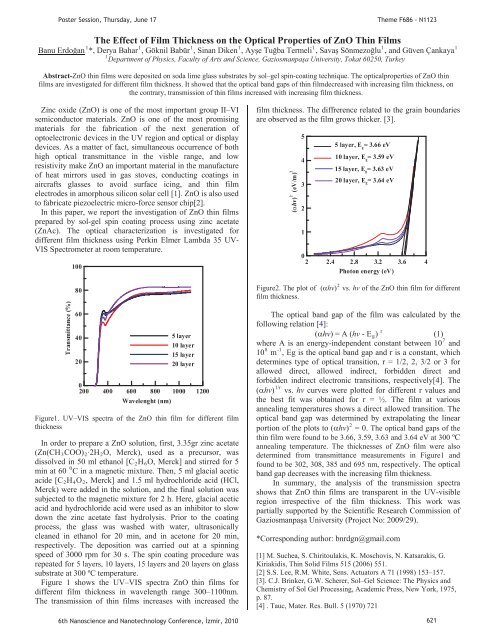
Figure1. UV–<strong>VI</strong>S spectra of the ZnO thin film for different film<br />
thickness<br />
In order to prepare a ZnO solution, first, 3.35gr zinc acetate<br />
(Zn(CHR3RCOO)R2R·2HR2RO, Merck), used as a precursor, was<br />
dissolved in 50 ml ethanol [CR2RHR6RO, Merck] and stirred for 5<br />
0<br />
min at 60 P PC in a magnetic mixture. Then, 5 ml glacial acetic<br />
acide [CR2RHR4ROR2R, Merck] and 1.5 ml hydrochloride acid (HCl,<br />
Merck) were added in the solution, and the final solution was<br />
subjected to the magnetic mixture for 2 h. Here, glacial acetic<br />
acid and hydrochloride acid were used as an inhibitor to slow<br />
down the zinc acetate fast hydrolysis. Prior to the coating<br />
process, the glass was washed with water, ultrasonically<br />
cleaned in ethanol for 20 min, and in acetone for 20 min,<br />
respectively. The deposition was carried out at a spinning<br />
speed of 3000 rpm for 30 s. The spin coating procedure was<br />
repeated for 5 layers, 10 layers, 15 layers and 20 layers on glass<br />
substrate at 300 ºC temperature.<br />
Figure 1 shows the UV–<strong>VI</strong>S spectra ZnO thin films for<br />
different film thickness in wavelength range 300–1100nm.<br />
The transmission of thin films increases with increased the<br />
film thickness. The diffrerence related to the grain boundaries<br />
are observed as the film grows thicker. [3].<br />
(hv) 2 (eV/m) 2<br />
5<br />
4<br />
3<br />
2<br />
1<br />
5 layer, E g<br />
= 3.66 eV<br />
10 layer, E g<br />
= 3.59 eV<br />
15 layer, E g<br />
= 3.63 eV<br />
20 layer, E g = 3.64 eV<br />
0<br />
2 2.4 2.8 3.2 3.6 4<br />
Photon energy (eV)<br />
2<br />
Figure2. The plot of (hv)P P vs. hv of the ZnO thin film for different<br />
film thickness.<br />
The optical band gap of the film was calculated by the<br />
following relation [4]:<br />
r<br />
(hv) = A (hv - ERgR) P<br />
7<br />
where A is an energy-independent constant between 10P<br />
8 -1<br />
10P<br />
P, Eg is the optical band gap and r is a constant, which<br />
determines type of optical transition, r = 1/2, 2, 3/2 or 3 for<br />
allowed direct, allowed indirect, forbidden direct and<br />
forbidden indirect electronic transitions, respectively[4]. The<br />
1/r<br />
(hv)P hv curves were plotted for different r values and<br />
the best fit was obtained for r = ½. The film at various<br />
annealing temperatures shows a direct allowed transition. The<br />
optical band gap was determined by extrapolating the linear<br />
2<br />
portion of the plots to (hv)P 0. The optical band gaps of the<br />
thin film were found to be 3.66, 3.59, 3.63 and 3.64 eV at 300 ºC<br />
annealing temperature. The thicknesses of ZnO film were also<br />
determined from transmittance measurements in Figure1 and<br />
found to be 302, 308, 385 and 695 nm, respectively. The optical<br />
band gap decreases with the increasing film thickness.<br />
In summary, the analysis of the transmission spectra<br />
shows that ZnO thin films are transparent in the UV-visible<br />
region irrespective of the film thickness. This work was<br />
partially supported by the Scientific Research Commission of<br />
Gaziosmanpaa University (Project No: 2009/29).<br />
*Corresponding author: bnrdgn@gmail.com<br />
[1] M. Suchea, S. Chiritoulakis, K. Moschovis, N. Katsarakis, G.<br />
Kiriakidis, Thin Solid Films 515 (2006) 551.<br />
[2] S.S. Lee, R.M. White, Sens. Actuators A 71 (1998) 153–157.<br />
[3]. C.J. Brinker, G.W. Scherer, Sol–Gel Science: The Physics and<br />
Chemistry of Sol Gel Processing, Academic Press, New York, 1975,<br />
p. 87.<br />
[4] . Tauc, Mater. Res. Bull. 5 (1970) 721<br />
6th Nanoscience and Nanotechnology Conference, zmir, <strong>2010</strong> 621


