

Third Day Poster Session, 17 June 2010 - NanoTR-VI
Third Day Poster Session, 17 June 2010 - NanoTR-VI
Third Day Poster Session, 17 June 2010 - NanoTR-VI

Create successful ePaper yourself
Turn your PDF publications into a flip-book with our unique Google optimized e-Paper software.
<strong>Poster</strong> <strong>Session</strong>, Thursday, <strong>June</strong> <strong>17</strong><br />
Theme F686 - N1123<br />
Fabrication of Micro Channels with Angled Sidewall on Silicon by Nd:YAG Laser Ablation<br />
Alperen Acemoglu, 1 Veysel Ozkapici 2,* ,Vural Kara 1 ,Omid Tayafeh 3 ,Huseyin Kizil 4 and Levent Trabzon 1,*<br />
1 Department of Mechanical Engineering, Istanbul Technical University, Gumussuyu, Istanbul 34437, Turkey<br />
2 BNM Fabrika Biyo Nano Mikro Tek. San. Ve Tic. Ekinciler Cad. 7/4 stanbul 34830, Turkey<br />
3 Department of Electronics and Communication Engineering, Istanbul Technical University, Maslak, Istanbul 34469, Turkey<br />
4 Department of Metallurgical and Materials Engineering, Istanbul Technical University, Maslak, Istanbul 34469, Turkey<br />
Abstract— We present experimental results on microfabrication of micro channels with angled sidewall on silicon surface by Nd:YAG laser.<br />
The purpose is to create V-shaped deep micro channels on silicon surface for producing nano-sharp micro Si-knife. The results can be used to<br />
characterize the behavior of ablation process under different laser parameters to achieve optimal processing conditions for Si-micromicromaching<br />
in MEMS such as V-shaped channels, slots and singulation process of vias.<br />
Micro channels on silicon wafer play an important role in<br />
many MEMS and NEMS applications. There are several<br />
microfabrication processes for creating proper micro channels<br />
on silicon surface. Conventional chemical and mechanical<br />
processes like etching, engraving and sawing have been<br />
successfully applied on to fabrication of micro channels [1, 2].<br />
Although well developed and mature production process, they<br />
are not suitable for all kind of MEMS application. That’s why<br />
laser are widely used to create this kind of channels on<br />
material, laser fabrication process is a non contact process<br />
therefore preferred in our task.<br />
Lasers are a powerful tool for micromachining<br />
applications. A focused laser beam can easily be concentrated<br />
onto a small target of a few micron diameters. The laser<br />
material-interaction in this target area will be controlled by<br />
laser parameters such as wavelength, pulse energy and pulse<br />
duration which determine peak power density [3]. Certain sets<br />
of parameters can cause thermal effects for marking, cutting,<br />
and drilling.<br />
In our work, we have specially chosen to work with<br />
Nd:YAG DPSS laser which has 1064 nm wavelength and 60<br />
W maximum power. There were limited survey on that, most<br />
of the laser on literature was in the UV range with either<br />
femto- or pico-seconds system, which are very expensive. Our<br />
main focus was creating those micro channels by nanosecond<br />
laser with a wavelength of 1064 nm.<br />
One of the important findings in the study is to have U-<br />
shaped channels with laser beam directed on the Si-wafer<br />
perpendicular. This observation is defined as tapering affect<br />
and it depends on the repletion of the laser ablation and depth<br />
of the channel produced in the ablation process [5]. Tapering<br />
affect is around 30°- 40° for 10 – 50 μm deep channels and<br />
they are roughly V-shaped channel as shown in Fig. 2a.<br />
Tapering affect was reduced to 10 °- 15° when channel depth<br />
is in between 51 and 150 μm.<br />
Main aim of this work is to create angled sidewall<br />
production on silicon wafer by laser. Then, we examined laser<br />
beam ablation on Si-wafer by different angles with laser beam.<br />
By means of adjustable wedge, the Si is oriented as 30°-45°-<br />
60° degree with respect to incoming laser in order to see<br />
sidewall affect and channel-wall angles. The channel-wall<br />
angles should be 30°-45°-60° degrees after inclined Si-wafer<br />
ablation by laser if there is no tapering effect. We measured<br />
channel-wall angles by profilometer on each Si wafer ablated<br />
by a different angle. We found that the channel-wall angles are<br />
38°-42°, 29°-34° and 19°-22° for ideally expected sidewall<br />
angel 60°, 45° and 30°, respectively. The difference between<br />
measured and expected angles is due to tapering effect in Si<br />
laser ablation.<br />
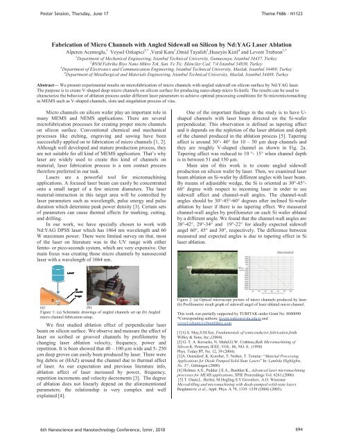
(a)<br />
(b)<br />
Figure 1: (a) Schematic drawings of angled channels set up (b) Angled<br />
micro channel fabrication setup.<br />
We first studied ablation effect of perpendicular laser<br />
beam on silicon surface. We observe and measure the effect of<br />
laser on scribed or grooved channels by profilometre by<br />
changing laser ablation velocity, frequency, power and<br />
repetition. It is been showed that 40 – 100 μm wide and 5- 250<br />
μm deep groves can easily been produced by laser. There were<br />
big debris or (HAZ) around the channel due to thermal affect<br />
of laser. As our expectation and previous literature info,<br />
ablation affect of laser increased by power, frequency,<br />
repetition increments and velocity decrements [3]. The degree<br />
of ablation does not linearly depend on the aforementioned<br />
parameters; the relationship is very complex and well<br />
explained [4].<br />
Figure 2: (a) Optical microscope picture of micro channels produced by laser<br />
(b) Profilometre result graph of sidewall angel of laser ablated micro channel.<br />
This work was partially supported by TUBITAK under Grant No. 8080090<br />
*Corresponding authors: levent.trabzon@itu.edu.tr and<br />
veysel.ozkapici@bnmfabric.com<br />
[1] G.S. May,S.M.Sze, Fundamentals of semiconductor fabrication,Jonh<br />
Willey & Sons, Inc.,(2004).<br />
[2] G. T. A. Kovacks, N. Maluf,G.W. Crabtree,Bulk Micromachining of<br />
Silicon K. Petersen, IEEE, VOL. 86, NO. 8, (1998)<br />
Phys. Today 57, No. 12, 39 (2004).<br />
[3]A. Ostendorf, K. Koerber, T. Nether, T. Temme: “Material Processing<br />
Applications for Diode Pumped Solid State Lasers” In: Lambda Highlights,<br />
No. 57 , Göttingen (2000)<br />
[4] Holmes A.S., Pedder J.E.A., Boehlen K., Advanced laser micromachining<br />
processes for MEMS applications, SPIE Proceedings Vol. 6261,(2006)<br />
[5] T. Otani,L. Herbst, M.Hegling.S.V.Govorkov, A.O. Wiessner<br />
Microdrilling and micromachining with diode-pumped solid-state lasers<br />
Bogdanovic et al., Appl. Phys. A 79, 1335–1339 (2004) (2003).<br />
6th Nanoscience and Nanotechnology Conference, zmir, <strong>2010</strong> 694


