

Third Day Poster Session, 17 June 2010 - NanoTR-VI
Third Day Poster Session, 17 June 2010 - NanoTR-VI
Third Day Poster Session, 17 June 2010 - NanoTR-VI

You also want an ePaper? Increase the reach of your titles
YUMPU automatically turns print PDFs into web optimized ePapers that Google loves.
<strong>Poster</strong> <strong>Session</strong>, Thursday, <strong>June</strong> <strong>17</strong><br />
Theme F686 - N1123<br />
Plasmonics: Novel On-Chip Interconnections<br />
Abstract— We report antenna designs for surface plasmon polariton coupling to metal-insulator-metal waveguides. The<br />
resulting plasmonic modes were tuned for maximum propagation length along the waveguide: for 1550 nm, we have observed<br />
more than 40 micron propagation (along the length of the waveguide, +x direction) while for 532 nm this is below 10 micron.<br />
Our results lay the foundations for on-chip coupler-waveguide-photodetector interconnect technology.<br />
State-of-the-art on-chip and chip-to-chip technologies rely<br />
on copper interconnects. Ever increasing data transfer rates<br />
and Moore’s Law dictate smaller devices packed into the same<br />
area [1]. Besides, International Technology Roadmap for<br />
Semiconductor Industry reports project devices that process<br />
and transmit data faster. Interconnections, not chips, have<br />
become the limiting factor for the future of scaling. Copper<br />
interconnects cannot meet the demanding data transfer rate<br />
requirements and have significant bandwidth limitations due<br />
to RC time delays, resistive losses, and frequency dependent<br />
cross-talk at high modulation frequencies. In addition to these<br />
limitations, electronic information transmission on a chip also<br />
suffer from impedance mismatch. On the device side, there is<br />
a high impedance and low capacitance, while transmission<br />
lines have low impedance and high capacitance. This<br />
mismatch limits the power transfer, even for the optimum<br />
cases [2-4].<br />
The incident light’s polarization significantly changes the<br />
coupling efficiency. Because antennas couple SPP’s to the<br />
waveguides in the near-field, the distance between the antenna<br />
and the waveguide was kept smaller than 50 nm. The antenna<br />
should not be connected to the waveguide either; otherwise<br />
interference of plasmonic modes reduces propagation length.<br />
Antenna and waveguide parameters were swept and the field<br />
profiles were compared for metal layer thicknesses of 100,<br />
150 and 200 nm. The longest propagation length has been<br />
achieved for 200 nm, while above 200 nm, the propagation<br />
length is no longer enhanced by changing the thickness.<br />
Thinner arms (60nm) tend to propagate SPP’s over longer<br />
distances. Reducing antenna gap enhanced local field between<br />
the arms, but did not increase the propagation length.<br />
Surface plasmon polaritons (SPP) are collective electron<br />
oscillations along the interface of metal and a dielectric.<br />
Because of the fast decaying fields both inside the metal and<br />
the dielectric, the mode field profile is highly confined along<br />
the interface. That is why; SPP’s can be a solution for<br />
achieving high integration densities, due to the small<br />
attenuation lengths, i.e. 14 nm as our simulations show. SPP’s<br />
are proposed to be the data transfer medium for on-chip<br />
clocking and signaling. The proposed geometry for<br />
transferring SPP’s is a metal-insulator-metal (MIM)<br />
waveguide structure where coupled SPP’s propagate along the<br />
two metal-insulator interfaces over long distances.<br />
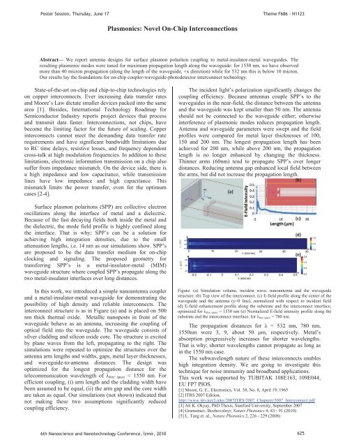
In this work, we introduced a simple nanoantenna coupler<br />
and a metal-insulator-metal waveguide for demonstrating the<br />
possibility of high density and reliable interconnects. The<br />
interconnect structure is as in Figure (a) and is placed on 500<br />
nm thick thermal oxide. Metallic nanoposts in front of the<br />
waveguide behave as an antenna, increasing the coupling of<br />
optical field into the waveguide. The waveguide consists of<br />
silver cladding and silicon oxide core. The structure is excited<br />
by plane waves from the left, propagating to the right. The<br />
simulations were repeated to optimize the structures over the<br />
antenna arm lengths and widths, gaps, metal layer thicknesses,<br />
and waveguide-to-antenna distances. The design was<br />
optimized for the longest propagation distance for the<br />
telecommunication wavelength of free space = 1550 nm. For<br />
efficient coupling, (i) arm length and the cladding width have<br />
been assumed to be equal, (ii) the arm gap and the core width<br />
are taken as equal. Our simulations (not shown) indicated that<br />
not making these two assumptions significantly reduced<br />
coupling efficiency.<br />
Figure: (a) Simulation volume, incident wave, nanoantenna and the waveguide<br />
structure. (b) Top view of the interconnect. (c) E-field profile along the center of the<br />
waveguide and the antenna (y=0 line), normalized with respect to incident field<br />
(d) E-field enhancement profile along the substrate and the interconnect interface,<br />
optimized for free space = 1550 nm (e) Normalized E-field intensity profile along the<br />
substrate and the interconnect interface, for free space = 780 nm.<br />
The propagation distances for = 532 nm, 780 nm,<br />
1550nm were 3, 9, about 50 μm, respectively. Metal’s<br />
absorption progressively increases for shorter wavelengths.<br />
That is why; shorter wavelengths cannot propagate as long as<br />
in the 1550 nm case.<br />
The subwavelength nature of these interconnects enables<br />
high integration density. We are going to investigate this<br />
technique for noise immunity and broadband applications.<br />
This work was supported by TUBITAK 108E163, 109E044,<br />
EU FP7 PIOS.<br />
[1] Moore, G. E., Electronics, Vol. 38, No. 8, April 19, 1965<br />
[2] ITRS 2007 Edition,<br />
http://www.itrs.net/Links/2007ITRS/2007_Chapters/2007_Interconnect.pdf<br />
[3] Ali K. Okyay, PhD Thesis, Stanford University, September 2007<br />
[4] Gramotnev, Bozhevolnyi; Nature Photonics 4, 83 - 91 (<strong>2010</strong>)<br />
[5] L. Tang et. al., Nature Photonics 2, 226 - 229 (2008)<br />
6th Nanoscience and Nanotechnology Conference, zmir, <strong>2010</strong> 625


