Third Day Poster Session, 17 June 2010 - NanoTR-VI
Third Day Poster Session, 17 June 2010 - NanoTR-VI
Third Day Poster Session, 17 June 2010 - NanoTR-VI
You also want an ePaper? Increase the reach of your titles
YUMPU automatically turns print PDFs into web optimized ePapers that Google loves.
P<br />
P for<br />
P for<br />
P edit.<br />
P<br />
<strong>Poster</strong> <strong>Session</strong>, Thursday, <strong>June</strong> <strong>17</strong><br />
Theme F686 - N1123<br />
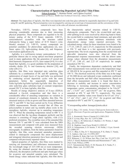
Characterization of Sputtering Deposited AgGaSe2 Thin Films<br />
1<br />
1<br />
1<br />
UHakan KaraaaçUP P*, Mehmet ParlakP Pand Çidem ErçelebiP<br />
1<br />
PDepartment of Physics, Middle East Technical University, Ankara 06531, Turkey<br />
Abstract- The single phase of AgGaSeR2R thin films were deposited onto soda-lime glass substrate by sequentially deposition of Ag and GaSe<br />
using DC and RF sputtering. Physical properties were investigated by carrying out several type of measurements and the convenience of this<br />
material to be used in the solar cell structure was determined.<br />
Nowadays, I-III-<strong>VI</strong>R2R ternary compounds have been<br />
attracting considerable attention due to their interesting<br />
physical properties. These compounds are regarded to be the<br />
ternary analog of the II-<strong>VI</strong> binary materials. I-III-<strong>VI</strong>R2R<br />
semiconductors crystallize with the structure called<br />
chalcopyrite being a super lattice of II-<strong>VI</strong> binary’s (zinc<br />
blende) structure [1]. I-III-<strong>VI</strong>R2R ternary compounds are<br />
potential candidates for photovoltaic applications [2], nonlinear<br />
optics [3], light-emitting diodes [4], and frequency<br />
conversation applications [5].<br />
AgGaSeR2R is a well-known ternary semiconductor. It’s of<br />
particular interest due to owing optical non-linear properties<br />
used in many applications like the generation of second and<br />
third harmonic frequencies of COR2R laser output [6-8]. It is also<br />
found that AgGaSeR2R is a good candidate for the preparation of<br />
schottky diodes [9], X- and Gamma-ray detector [10], and<br />
solar cells [11].<br />
AgGaSeR2R thin films were deposited onto soda-lime glass<br />
substrates by a combination of DC and RF sputtering. The<br />
optimization of single layers of Ag and GaSe was performed<br />
by conducting several deposition cycles with the same<br />
parameters before the sequentially deposition of<br />
GaSe/Ag/GaSe/Ag/GaSe/Ag/GaSe/Ag/GaSe thin film layers<br />
onto soda-lime glass substrates kept at constant temperature<br />
o<br />
around 250 P PC to form AgGaSeR2R thin film.<br />
Results of energy dispersive analysis of X-rays (EDXA)<br />
indicated a Ga-rich composition and that there is a<br />
considerable effect of annealing temperature on variation in<br />
amount of constituent elements in AgGaSeR2R thin film. The<br />
structural analysis of the as-grown and films annealed between<br />
o<br />
o<br />
350 P PC and 600 P PC has been carried out by X-ray diffraction<br />
(XRD) measurements. Results revealed that all films are<br />
polycrystalline in nature and Ag metallic phase exists in the<br />
amorphous AgGaSeR2R structure up to annealing temperature<br />
o<br />
o<br />
450 P PC. When the annealing temperature raised to 600 P PC it<br />
was observed that the Ag phase disappears perfectly and the<br />
structure is consisting of single phase AgGaSeR2R with (112)<br />
preferred orientation. The crystalline sizes of the annealed film<br />
o<br />
o<br />
between 350 P PC and 600 P PC were calculated from the XRD<br />
measurements and compared with grain sizes measured from<br />
the recorded scanning electron microscopy (SEM)<br />
micrographs. In addition, from the lattice parameters found for<br />
AgGaSeR2R thin film, some structural anomalies parameters<br />
related to chalcopyrite compounds like anion displacement<br />
and tetragonal distortion parameters have been calculated and<br />
compared with previously reported values.<br />
Optical properties of AgGaSeR2R thin films were studied by<br />
carrying out transmittance and reflectance measurements in<br />
the wavelength range of 325-1100 nm at room temperature.<br />
By using the obtained spectral data for transmittance and<br />
reflection, the absorption coefficient and optic band gap values<br />
for as-grown and annealed samples were calculated. The<br />
found energy values indicated that AgGaSeR2R thin film shows<br />
the characteristic optical structure related to I-III-<strong>VI</strong>R2R<br />
chalcopyrite compounds. That’s the crystal-field and spinorbit<br />
splitting levels were resolved by observing band to band,<br />
the crystal-field to conduction band minimum, and spin-orbit<br />
level to conduction band minimum transitions with<br />
characteristic energy values reported previously. The<br />
calculated energy values for these transitions were found to be<br />
1.77 eV, 2.00 eV, and 2.25 eV, respectively for film annealed<br />
o<br />
at 550 P PC and there is a fair agreement with previously<br />
reported data. The levels originating from the crystal-field and<br />
spin-orbit interaction were also observed from the<br />
photospectral response measurements with the almost same<br />
energy values obtained from the absorption measurements<br />
(1.77 eV, 2.00 eV, and 2.25 eV respectively for sample<br />
o<br />
annealed at 550 P PC).<br />
Finally, the temperature dependent conductivity and Hall<br />
effect measurements were carried out in the temperature range<br />
o<br />
of 100-430 K for as-grown and film annealed at 450 P PC and<br />
o<br />
550 P PC. The electrical resistivity of the films was in the range<br />
of 30-1000 -cm and indicated n-type conduction confirmed<br />
from the hot-probe and Hall effect measurements. Based on<br />
Hall effect measurement results it is found that there is<br />
decrease in mobility and increase in carrier concentration<br />
following to increasing annealing temperature. The room<br />
14<br />
temperature carrier concentration calculated to be 9.6x10P<br />
-3<br />
15 -3<br />
16 -3<br />
cmP<br />
P, 1.7x10P<br />
P cmP<br />
P, and 6.6x10P<br />
P cmP as-grown, films<br />
o<br />
o<br />
annealed at 450 P PC and 550 P PC, respectively. The room<br />
2 -1<br />
temperature mobility values were found to be 6.4 cmP P (Vs)P<br />
P,<br />
2 -1<br />
2 -1<br />
3.7 cmP P (Vs)P<br />
P, and 3 cmP P (Vs)P as-grown and films<br />
o<br />
o<br />
annealed at 450 P PC and 550 P PC, respectively.<br />
*Corresponding author: karaagac@metu.edu.tr<br />
[1] J. L. Shay, J. H. wernic, Ternary Chalcopyrite Semiconductors,<br />
Growth, Electronic Properties and Applications, Pergamon, Oxford,<br />
1975<br />
[2] L. L. Kazmerski, Nuovo Cimento D 2 (1983) 2013<br />
[3] B. F. Levine, Phys. Rev. B, 7 (1973) 2600<br />
[4] J. L. Shay, L. M. Schiavone, E. Buehier, J. H. Wernic, J. Appl.<br />
Phys. 43 (1972) 2805<br />
[5] F. K. Hopkius, Laser Focus World 31 (1995) 87<br />
[6] P. G. Schunemann, S. D. Setzler, T. M. Pollak, J. Cryst. Growth<br />
211 (2000) 257<br />
[7] G. C. Bhar, S. Das, D. V. Satyanarayan, P. K. Datta, U. Nundy,<br />
Y. N. Andreev, Opt. Lett. 15 (1995) 2057<br />
[8] E. Takaoka, K. Kato, Opt. Lett. 24 (1999) 902<br />
[9] P. Ribinson, J. I. B. Wilson, Inst. Phys. Conf. Ser. 35 (1977) 229<br />
rd<br />
[10] G. F. Knoll, Radiation detection and Measurement 3P<br />
(New-York; Willey), (1999)<br />
[11] Y. Satyanarayana Murty, O. M. Hussain, B. S. Naidu, P. J.<br />
Reddy, Mater. Lett. 10 (1987) 504<br />
6th Nanoscience and Nanotechnology Conference, zmir, <strong>2010</strong> 754


