

Third Day Poster Session, 17 June 2010 - NanoTR-VI
Third Day Poster Session, 17 June 2010 - NanoTR-VI
Third Day Poster Session, 17 June 2010 - NanoTR-VI

Create successful ePaper yourself
Turn your PDF publications into a flip-book with our unique Google optimized e-Paper software.
<strong>Poster</strong> <strong>Session</strong>, Thursday, <strong>June</strong> <strong>17</strong><br />
Theme F686 - N1123<br />
CRYSTALLIZATION OF THIN Si FILM FABRICATED BY ELECTRON BEAM<br />
EVAPORATION ON GLASS SUBSTRATE FOR SOLAR CELLL APPLICATIONS<br />
M. Karaman a , Ö. Tüzün b , R. Turan a , . Oktik b<br />
a Department of Physics, Middle East Technical University, 06531 Ankara, Turkey<br />
b Department of Physics, Mula University, 48000 Mula, Turkey<br />
E-Mail: mkaramanm@gmail.com<br />
Abstract<br />
Amorphous, nanocrystalline and<br />
polycrystalline silicon thin films fabricated<br />
on glass substrate are of great interest for<br />
low-cost and high efficiency solar cells.<br />
There are various techniques to fabricate<br />
such kind of cells[1]. Solid Phase<br />
Crystallization (SPC) technique is<br />
favourable due to its easy production and<br />
resulting high quality, such as larger<br />
grained, less defective thin films. However,<br />
its long crystallization annealing is the<br />
disadvatage for industrial production<br />
application[2]. This important problem is<br />
solved by a novel annealing technique that<br />
consists of two-step annealing. These are<br />
low-temperature annealing (475 o C for 8h) to<br />
start the nucleation with a lower nucleation<br />
rate and high-temperature annealing (900 o C<br />
for 1h) to reduce the annealing time<br />
dramatically. In this approach, novel SPC<br />
process results larger grain size with lower<br />
defects compared to conventional lowtemperature<br />
SPC process while the hightemperature<br />
annealing reduces the<br />
crystallization time. This two step annealing<br />
processes lead to a phase transformation<br />
from a fully amorphous phase to a<br />
nanocrystalline phase and finally a<br />
polycrystalline phase in the film. This work<br />
aims to undertand the basic kintics in these<br />
transformation processes.<br />
Ex situ doped amorphous silicon is<br />
deposited by electron beam evaporation<br />
system with a depositon rate of 3Å/sec, and<br />
crystallized by classical thermal process.<br />
The structural analysis of the films formed<br />
by this novel annealing process is analyzed<br />
by optical microscopy, scanning electron<br />
microscopy (SEM), electron back scattering<br />
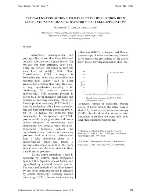
diffraction (EBSD) technique, and Raman<br />
Spectroscopy. Raman spectroscopy allowed<br />
us to monitor the crystallinity of the grown<br />
layer. It also provided infromation about the<br />
Figure1. Raman measurement after 475°C 8h+900°C<br />
60min annealing process<br />
structures formed at nanoscale. Doping<br />
profile of boron through the active layer is<br />
studied by secondary ion mass spectroscopy<br />
(SIMS). Results show that structures with<br />
nanometer dimension are observable even<br />
after high temeparture annealings.<br />
[1] T. Baba, M. Shima, T. Matsuyama, S. Tsuge, K.<br />
Wakisaka, S. Tsuda, In: Proc. 13 th European Photovoltaic<br />
Solar Energy Conf. (1995) <strong>17</strong>08.<br />
[2] T. Baba, T. Matsuyama, T. Sawada, T. Takahama, K.<br />
Wakisaka, S. Tsuda, MRS Symp. Proc. 358 (1995) 895<br />
<br />
<br />
6th Nanoscience and Nanotechnology Conference, zmir, <strong>2010</strong> 768


