

Third Day Poster Session, 17 June 2010 - NanoTR-VI
Third Day Poster Session, 17 June 2010 - NanoTR-VI
Third Day Poster Session, 17 June 2010 - NanoTR-VI

You also want an ePaper? Increase the reach of your titles
YUMPU automatically turns print PDFs into web optimized ePapers that Google loves.
P<br />
is<br />
P<br />
P<br />
is<br />
is<br />
is<br />
P,P<br />
is<br />
<strong>Poster</strong> <strong>Session</strong>, Thursday, <strong>June</strong> <strong>17</strong><br />
Theme F686 - N1123<br />
Photoluminescent Properties of InN Thin Films<br />
1<br />
2<br />
1<br />
2<br />
1<br />
2<br />
3<br />
3<br />
UÖ. DönmezUP P*, M. YlmazP P, A. ErolP P, B. UluP P, M.Ç. ArkanP P, A. UluP<br />
PA. O. AjagunnaP P, E. IliopoulosP P, A. GeorgakilasP<br />
1<br />
PIstanbul University, Science Faculty, Department of Physics 34134 Vezneciler, Istanbul, Turkey<br />
2<br />
PAkdeniz University, Faculty of Arts & Science, Department of Physics, Antalya, Turkey<br />
PMicroelectronics Research Group, IESL, FORTH and Physics Department, University of Crete, P.O. Box 1385, 71110 Heraklion-Crete, Greece<br />
3<br />
Abstract-We report photoluminescence (PL) studies of InN epilayers grown by plasma-assisted molecular beam epitaxy with free-electron<br />
19 -3<br />
concentration of about 10P<br />
PcmP P. Band gap of InN layer is determined using the PL data obtained as a function of temperature and is calculated<br />
by a model considering the high electron concentration effect, electron-electron and electron-ionized impurity interactions in non-parabolic k·p<br />
model. PL results indicate that the band gap of InN is 0.82eV at 8K. Electron effective mass is calculated as 0.097mR0 Rfor electron concentration<br />
19 -3<br />
of 10P<br />
PcmP<br />
3<br />
InN is in nature n-type semiconductor having free-electron<br />
21 -3<br />
concentrations as high as 10P<br />
PcmP<br />
P. Early studies of the<br />
interband optical absorption carried out on InN thin films have<br />
shown that band gap energy is about 2eV due to high carrier<br />
concentration effects [1-2]. Recent studies showed that the<br />
band gap energy is about 0.65eV [3-6]. This means that using<br />
group InN and In-rich InGaN have potential to optoelectronic<br />
devices covering the spectrum from infrared to ultraviolet.<br />
In this study, Hall effect measurement has employed to<br />
determine carrier concentration for two samples having<br />
different InN layer thicknesses as shown in Figure 1.<br />
Carrier Conc.(cm -3 )<br />
1,4E19<br />
1,3E19<br />
1,2E19<br />
1,1E19<br />
800nm InN layer<br />
600nm InN layer<br />
1E19<br />
60 90 120 150 180 210 240 270 300<br />
Temperature (K)<br />
Figure 1. Temperature dependence of carrier concentration of 800 nm<br />
and 600 nm thick InN layers<br />
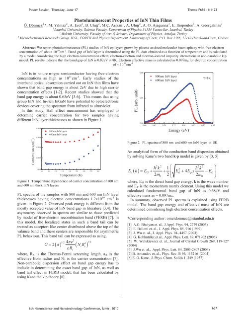
PL spectra of the samples with 800 nm and 600 nm InN layer<br />
19 -3<br />
thicknesses having electron concentrations 1.2x10P<br />
P cmP<br />
Pis<br />
given in Figure 2. Observed peak energy is different from the<br />
mostly accepted value of InN band gap in literature [3,4]. The<br />
asymmetry observed in spectra are similar to those predicted<br />
by model of free-electron recombination band (FERB) [7]. In<br />
this model, the localized states in such a band tail can be<br />
treated as acceptor- like center distributed above the top of the<br />
valance band and these centers are responsible for asymmetric<br />
PL behaviour. This band tail can be expressed as using,<br />
2<br />
1/2 4<br />
e 3<br />
1/2<br />
G 2<br />
NiR<br />
s <br />
Rs<br />
where, RRSR the Thomas-Fermi screening length, aRBR the<br />
effective Bohr radius and NRR the carrier concentration [7].<br />
Non-parabolic dispersion effect on band gap energy has to<br />
include in determining the exact band gap of InN, as well as<br />
band tail effect in FERB model, that has been calculated by<br />
using Kane the k·p theory [8].<br />
PL (arb. unit)<br />
0,08<br />
0,04<br />
800nm InN layer<br />
600nm InN layer<br />
0,00<br />
0,60 0,65 0,70 0,75 0,80 0,85 0,90 0,95<br />
Energy (eV)<br />
T=8K<br />
Figure 2. PL spectra of 800 nm and 600 nm InN layer at 8K<br />
An analytical form of the conduction band dispersion obtained<br />
by solving Kane’s two band k·p model is given by [3, 5]<br />
2 2 2 2<br />
k 1 <br />
2 k <br />
Eck EG EG 4Epx EG<br />
2m0 2<br />
2m<br />
<br />
<br />
0 <br />
where, ERGR the direct band gap energy, k is the wave number<br />
and ERPR the momentum matrix element. Using this model we<br />
calculated fundamental band gap of InN as 0.68eV and<br />
effective mass as ~ 0.097mR0R.<br />
In summary, observed PL spectra is explained using FERB<br />
model. The band gap energy and effective mass of InN are<br />
determined considering high electron concentration effects.<br />
*Corresponding author: omerdonmez@istanbul.edu.tr<br />
[1] A.G. Bhuiyan et. al., J.Appl. Phys. 94, 2779 (2003)<br />
[2] E. Bellotti et. al., J. Appl. Phys. 85, 916 (1999)<br />
[3] J. Wu et. al., J. Appl. Phys. T94T, 4457 (2003)<br />
[4] G. Koblmüller,et.al., Appl. Phys. Lett. 89, 071902 (2006)<br />
[5] W. Walukiewicz et. al., Journal of Crystal Growth 269, 119-127<br />
(2004)<br />
[6] J.Wu et. al., Appl. Phys. Lett. 84, 2805-2807 (2004)<br />
[7] B. Arnaudov et. al., Phys. Rev. B 69, 115216 (2004)<br />
[8] E. O. Kane , J. Phys. Chem. Solids 1, 249 (1957)<br />
6th Nanoscience and Nanotechnology Conference, zmir, <strong>2010</strong> 637


