

Third Day Poster Session, 17 June 2010 - NanoTR-VI
Third Day Poster Session, 17 June 2010 - NanoTR-VI
Third Day Poster Session, 17 June 2010 - NanoTR-VI

Create successful ePaper yourself
Turn your PDF publications into a flip-book with our unique Google optimized e-Paper software.
Ultraviolet light detection characteristics of a-IGZO thin film transistor for photodetector applications<br />
Seongpil Chang a , Jae-Hong Kwon a , Jung-Ho Park a , Myung-Ho Chung a , Tae-Yeon Oh a , Hyun-Seok Bae a , Byeong-<br />
Kwon Ju a,† , and Fahrettin Yakuphanoglu b<br />
a) Display and Nanosystem Laboratory, College of Engineering, Korea University, Seoul 136-713, Republic of Korea.<br />
b) Fırat University, Faculty of Arts and Sciences, Department of Physics, Elazığ, Turkey.<br />
Abstract— The ultraviolet light responsive properties of the amorphous indium gallium zinc oxide thin film transistor have been<br />
investigated. The a-IGZO transistor operate in the enhancement mode with saturation mobility of 6.99 cm 2 /V s, threshold voltage<br />
of 7.6 V, gate voltage swing of 1.58 V/dec and an ON/OFF current ratio of 2.45x10 8 . The transistor was subsequently<br />
characterized in respect of UV illuminations in order to investigate its potential for possible use as a detector. The performance of<br />
the transistor is indicates a high-photosensitivity in the off-state with a ratio of photocurrent to dark current of 5.74x10 2 . Our<br />
results reveal that the amorphous indium gallium zinc oxide thin film transistor can be used as a UV photodetector.<br />
Transparent oxide semiconductors, such as zinc oxide (ZnO),<br />
indium tin oxide (ITO), zinc tin oxide (ZTO), gallium doped<br />
zinc oxide (GZO) indium zinc oxide (IZO), and indium<br />
gallium zinc oxide (IGZO) have attracted many researchers<br />
with their great potential in optoelectronic applications such as<br />
flat panel displays, transparent electrodes in solar cells,<br />
transparent thin film transistors (TFTs), and flexible<br />
transparent TFTs [1-7]. Moreover a-IGZO thin film transistors<br />
can be used to detect the ultraviolet (UV). This property of a-<br />
IGZO thin film is very useful to apply the UV-detector. In<br />
present study, we fabricated a-IGZO thin film transistor to<br />
investigate the photo-sensing characteristics of the transistor<br />
under the illuminations of visible light and UV. Thermally<br />
oxidized p-Si (100, ρ=0.005 Ωcm) is used as substrate.<br />
Thermally oxidized SiO 2 of 300 nm is used as the gateinsulator.<br />
And then, we deposited a-IGZO thin film by using<br />
radio-frequency (RF) magnetron sputtering. Active layer is<br />
patterned by photolithography and lift-off process. As the<br />
source-drain (S/D) electrodes, molybdenum (Mo) of 100 nm is<br />
deposited by using direct-current (DC) sputtering at roomtemperature.<br />
Our devices have channel width (W) of 150 μm<br />
and channel length (L) of 20 μm. Fig.1 shows schematic<br />
diagram of a-IGZO TFT<br />
Mo (Source / Drain, 100 nm)<br />
a-IGZO (80 nm)<br />
-a-<br />
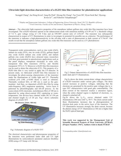
-b-<br />
Fig.2. Output characteristics of a-IGZO thin film transistor<br />
under dark and UV illuminations.<br />
Fig.2a shows the drain current-drain voltage characteristics<br />
of a-IGZO transistor under various gate voltages. The drain<br />
current increases at positive voltages, indicating that the<br />
electrons are generated by the positive gate voltages due to n-<br />
type FET characteristics with good gate controllability. The<br />
drain current of the transistor reaches a saturation region,<br />
when the entire channel region is depleted of electrons, i.e,<br />
channel is pinched off.<br />
Fig.2b shows the I ds -V ds curves obtained under UV<br />
illuminations (366 nm) with V g =30 V. The drain current under<br />
these illuminations increases due to photogeneration of<br />
electron–hole pairs in the active layer of the transistor. The<br />
UV illumination increases strongly the drain current, because<br />
the photon energy of UV illumination at 366 nm is higher than<br />
the IGZO optical band gap.<br />
SiO x (300 nm)<br />
p-Si (100 oriented, ρ=0.005 Ωcm)<br />
Ag (Gate Electrode)<br />
Fig.1 Schematic diagram of a-IGZO TFT<br />
The electrical characteristics and photoresponse properties of<br />
the transistor were performed under dark and UV light<br />
illuminations by semiconductor parameter analyzer (Keithley<br />
4200) using a UV lamp with 366 nm.<br />
This work was supported by the Management Unit of<br />
Scientific Research Projects of Firat University (FÜBAP)<br />
(Project Number: 1947). Authors wish to thank FÜBAP.<br />
*Corresponding author: fyhan@hotmail.com<br />
6th Nanoscience and Nanotechnology Conference, zmir, <strong>2010</strong> 1


