

Third Day Poster Session, 17 June 2010 - NanoTR-VI
Third Day Poster Session, 17 June 2010 - NanoTR-VI
Third Day Poster Session, 17 June 2010 - NanoTR-VI

Create successful ePaper yourself
Turn your PDF publications into a flip-book with our unique Google optimized e-Paper software.
<strong>Poster</strong> <strong>Session</strong>, Thursday, <strong>June</strong> <strong>17</strong><br />
Theme F686 - N1123<br />
Electrical and photosensing properties of pentacene organic thin film transistor<br />
Fahrettin Yakuphanoglu<br />
<br />
Abstract— The electrical and ultraviolet light responsive properties of the pentacene thin-film transistor with 240 nm poly-4-<br />
vinylphenol (PVP) dielectric layer thin film transistor have been investigated. The electrical parameters, saturation mobility,<br />
threshold voltage, gate voltage swing and an ON/OFF current ratio were determined to be 710 -1 cm 2 /V s, 10.0 V, 2.6 V/dec and<br />
3.8x10 2 , respectively. The transistor was characterized in respect of UV illuminations to investigate its potential for possible use as<br />
a UV detector. The performance of the transistor is indicates a UV photosensitivity in the off-state with a ratio of photocurrent to<br />
dark current of 5.74x10 2 . The obtained results indicate that the organic pentacene thin film transistor can be used as a UV<br />
photodetector.<br />
Organic thin-film transistors (OTFTs) have been extensively<br />
investigated due to their low-cost, low-temperature process,<br />
and compatibility with flexible substrate. Organic thin film<br />
transistors (OTFTs) have many unique advantages, such as<br />
light weight, flexibility, and solution processability. From<br />
these reasons, nowadays, many research groups have<br />
developed OTFTs. Especially, solution processes included<br />
spin coating, screen printing, ink jet, and nanoimprint<br />
lithography can be easily used in coating processes to form<br />
circuits for disposable electronics on a plastic substrate.<br />
According to the reported investigation of active channel<br />
pentacene is a very promising candidate for organic<br />
electronics. Several groups have recently demonstrated<br />
pentacene TFTs and their applications. However, to satisfy the<br />
high performance of OTFT, it is very important to select a<br />
gate insulator material. That is, an insulator gate field-effect<br />
transistor, the role of the insulator is at least as important as<br />
that of the semiconductor. The insulator layer, especially the<br />
insulator-semiconductor interface, has a significant effect on<br />
the performance of OTFTs, because OTFTs operate in<br />
accumulation region and the modulated charge lies within the<br />
area (about 10 nm thick) close to the interface [8]. Therefore,<br />
many research groups have made much effort to be study on<br />
relationship between organic semiconductor and dielectric<br />
layer.<br />
In present study, pentacene thin-film transistor was<br />
fabricated with 240 nm poly-4-vinylphenol (PVP) dielectric<br />
layer. The electrical and photosensing properties of organic<br />
pentacene thin-film transistor fabricated on polyethersulphone<br />
(PES) substrate have been investigated. The transistor<br />
fabricated on PES showed p-type OTFT characteristics. For<br />
photosensing characterization, the output characteristics of the<br />
pentacene thin film transistor were measured under various<br />
illumination conditions. The Electrical characteristics and<br />
photoresponse properties of the transistor were performed<br />
under dark and UV light illuminations by semiconductor<br />
parameter analyzer (Keithley 4200) using a white lamp (200<br />
W) and UV lamp with 366 nm.<br />
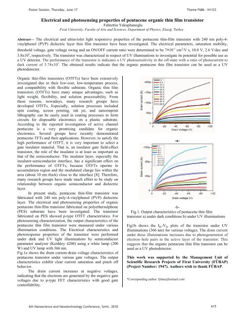
Fig.1a shows the drain current-drain voltage characteristics of<br />
pentacene transistor under various gate voltages. The output<br />
characteristics exhibit clear current saturation and pinch off<br />
behavior.<br />
The drain current increases at negative voltages,<br />
indicating that the electrons are generated by the negative gate<br />
voltages due to p-type FET characteristics with good gate<br />
controllability.<br />
-a-<br />
-b-<br />
Fig.1. Output characteristics of pentacene thin film<br />
transistor a) under dark conditions b) under UV illuminations<br />
Fig1b shows the I ds -V ds plots of the transistor under UV<br />
illuminations (366 nm) for various voltages. The drain current<br />
under these illuminations increases due to photogeneration of<br />
electron–hole pairs in the active layer of the transistor. This<br />
suggests that the organic pentacene thin film transistor can be<br />
used as a UV photodetector.<br />
This work was supported by the Management Unit of<br />
Scientific Research Projects of Firat University (FÜBAP)<br />
(Project Number: 1947). Authors wish to thank FÜBAP.<br />
*Corresponding author: fyhan@hotmail.com<br />
6th Nanoscience and Nanotechnology Conference, zmir, <strong>2010</strong> 615


