

Third Day Poster Session, 17 June 2010 - NanoTR-VI
Third Day Poster Session, 17 June 2010 - NanoTR-VI
Third Day Poster Session, 17 June 2010 - NanoTR-VI

You also want an ePaper? Increase the reach of your titles
YUMPU automatically turns print PDFs into web optimized ePapers that Google loves.
P<br />
P light<br />
<strong>Poster</strong> <strong>Session</strong>, Thursday, <strong>June</strong> <strong>17</strong><br />
Theme F686 - N1123<br />
ZnO/CuR2RO Inorganic Solar Cells<br />
1<br />
1<br />
1<br />
0BYakup HameP P, UTeoman ÖzdalUP P*, Hüseyin arP P, Erdem AslanP<br />
1P and Hüsnü nci 1<br />
P<br />
PMustafa Kemal University, Electric-Electronic Engineering Department, skenderun, Hatay, Turkey<br />
1<br />
Abstract -In this work thin film photovoltaic produced and investigated. Bilayer structured device has ZnO and CuR2RO inorganic oxide layers<br />
as n-type and p-type materials, respectively. Both oxide layers deposited by electrochemical deposition method on to pre cleaned Indium tin<br />
oxide (ITO) coated glass substrate. As a top electrode Al thermally coated and ITO/ZnO/CuR2RO/Al structure obtained. Finally, I-V curve of<br />
2<br />
thin film obtained and investigated by illumination under 100 mW/cmP intensity.<br />
There has been an active search for cost-effective<br />
photovoltaic devices since the development of the first solar<br />
cells in the 1950s [1]. A significant fraction of the cost of<br />
solar panels comes from the photoactive materials and<br />
sophisticated, energy-intensive processing technologies.<br />
Zinc oxide (ZnO), as a transparent conductive oxide, is one<br />
of the most attractive materials for last several decays. ZnO,<br />
has a wide field application for industrial and scientific<br />
researches due to transparent and conductive properties. ZnO<br />
has a big interest because of bandgap of 3.3 eV at T300 KT<br />
which is an advantage for Toptoelectronic applications.<br />
However, ZnO has large exiton-binding energy (T60 meV).<br />
ZnO thin films have attracted many researchers to work on<br />
because of its unique electrical, optical and acoustic<br />
characteristics that making it suitable for various fields of<br />
applications especially in photovoltaics [2]. ZnO films which<br />
deposited by ECD method generally obtain in aqueous alkali<br />
or neutral zinc salt solvents.<br />
Cuprous oxide (CuR2RO), as a non-toxic and active electrode<br />
has a big attractive for photovoltaic applications.<br />
CuR2RO semiconductor material has an ability to absorb visible<br />
wavelength with band-gap energy of 2,1 eV. Furthermore, it<br />
has been predicated that CuR2RO is promising for photovoltaic<br />
applications, with a theoretical energy conversion efficiency<br />
of 20% [3]. CuR2RO thin films have been prepared by various<br />
techniques like thermal oxidation, chemical vapor deposition<br />
(CVD), anodic oxidation, reactive sputtering, pulse laser<br />
deposition, electrodeposition, plasma oxidation [4-10].<br />
Cathodic electrodeposition of CuR2RO is a good method to<br />
control easily the particle size and the film thickness [11].<br />
ITO coated glass sonicated in acetone, 2-propanol, ethanol<br />
and pure water for 15 minutes respectively. Deposition of<br />
ZnO and CuR2RO obtained in a three electrode system. During<br />
the deposition, solution unstirred and temperature kept<br />
constant. Finally, Al top electrode thermally coated on to<br />
device as an ohmic contact.<br />
Electrical characterization of device obtained under 100<br />
2<br />
mW/cmP<br />
Plight intensity. Current-Voltage (IRSCR-VROCR)<br />
measurements of device obtained with Keithley 4200HT-TTSCSTT<br />
(semiconductor characterization systemTH). Scanning electron<br />
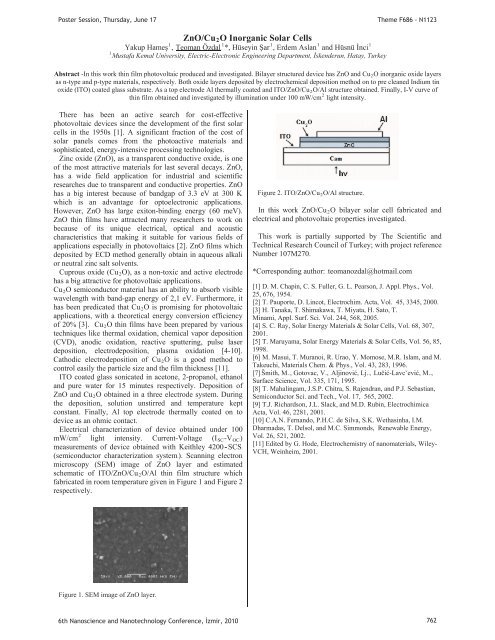
microscopy (SEM) image of ZnO layer and estimated<br />
schematic of ITO/ZnO/CuR2RO/Al thin film structure which<br />
fabricated in room temperature given in Figure 1 and Figure 2<br />
respectively.<br />
Figure 2. ITO/ZnO/CuR2RO/Al structure.<br />
In this work ZnO/CuR2RO bilayer solar cell fabricated and<br />
electrical and photovoltaic properties investigated.<br />
This work is partially supported by The Scientific and<br />
Technical Research Council of Turkey; with project reference<br />
Number 107M270.<br />
*Corresponding author: HTteomanozdal@hotmail.comT<br />
[1] D. M. Chapin, C. S. Fuller, G. L. Pearson, J. Appl. Phys., Vol.<br />
25, 676, 1954.<br />
[2] T. Pauporte, D. Lincot, Electrochim. Acta, Vol. 45, 3345, 2000.<br />
[3] H. Tanaka, T. Shimakawa, T. Miyata, H. Sato, T.<br />
Minami, Appl. Surf. Sci. Vol. 244, 568, 2005.<br />
[4] S. C. Ray, Solar Energy Materials & Solar Cells, Vol. 68, 307,<br />
2001.<br />
[5] T. Maruyama, Solar Energy Materials & Solar Cells, Vol. 56, 85,<br />
1998.<br />
[6] M. Masui, T. Muranoi, R. Urao, Y. Momose, M.R. Islam, and M.<br />
Takeuchi, Materials Chem. & Phys., Vol. 43, 283, 1996.<br />
[7]HTŠmith, M.TH, Gotovac, V., HTAljinovi, Lj.TH, HTLui-Lavcevi, M.TH,<br />
Surface Science, Vol. 335, <strong>17</strong>1, 1995.<br />
[8] T. Mahalingam, J.S.P. Chitra, S. Rajendran, and P.J. Sebastian,<br />
Semiconductor Sci. and Tech., Vol. <strong>17</strong>, 565, 2002.<br />
[9] T.J. Richardson, J.L. Slack, and M.D. Rubin, Electrochimica<br />
Acta, Vol. 46, 2281, 2001.<br />
[10] C.A.N. Fernando, P.H.C. de Silva, S.K. Wethasinha, I.M.<br />
Dharmadas, T. Delsol, and M.C. Simmonds, Renewable Energy,<br />
Vol. 26, 521, 2002.<br />
[11] Edited by G. Hode, Electrochemistry of nanomaterials, Wiley-<br />
VCH, Weinheim, 2001.<br />
Figure 1. SEM image of ZnO layer.<br />
6th Nanoscience and Nanotechnology Conference, zmir, <strong>2010</strong> 762


