

Third Day Poster Session, 17 June 2010 - NanoTR-VI
Third Day Poster Session, 17 June 2010 - NanoTR-VI
Third Day Poster Session, 17 June 2010 - NanoTR-VI

You also want an ePaper? Increase the reach of your titles
YUMPU automatically turns print PDFs into web optimized ePapers that Google loves.
U Neslihan<br />
P<br />
P<br />
P<br />
<strong>Poster</strong> <strong>Session</strong>, Thursday, <strong>June</strong> <strong>17</strong><br />
Theme F686 - N1123<br />
1<br />
3 Dimensional L Shaped Photonic Crystal Waveguide<br />
1<br />
1<br />
1<br />
EtiUP P*, H. Sami SözüerP PP and Zebih ÇetinP<br />
P<br />
Abstract- We present theoretical studies on waveguide bends in a combination of 1 dimensional and 2 dimensional photonic crystal slab.<br />
In this work, we give a method to bend light on L shaped photonic crystal waveguide slabs with little loss.<br />
1<br />
The discovery of the photonic crystal waveguides (PCWs),<br />
which allow only certain electromagnetic wave modes to<br />
propagate inside the structure, has opened up new ways of<br />
controlling light propagation in optical integrated circuit<br />
designs. By using photonic crystal slab waveguides, which<br />
are 1 dimensional or 2 dimensional periodic structures with a<br />
finite thickness in the vertical direction, it is possible to<br />
fabricate light guiding optical materials by total internal<br />
reflection [1], that confines light to the slab, and bend them<br />
with little loss by photonic crystal assistance.<br />
With conventional dielectric waveguides which depend<br />
entirely on total internal reflection, there is a problem in<br />
guiding light while turning through sharp edges and tight<br />
curves because the angle of the incidence is too high for total<br />
internal reflection, resulting in most of the electromagnetic<br />
field being radiated out and lost.<br />
To cope with this problem, a 2 dimensional line defect<br />
waveguide can be used [2-8]. The problem with 2<br />
dimensional line defect waveguides is that even small<br />
defects during manufacturing can greatly increase<br />
attenuation, thus limiting their usefulness to guide light over<br />
long distances. To overcome this difficulty, Notomi proposed<br />
using a 1 dimensional slab waveguide which is not periodic<br />
in the direction of propagation, to reduce dispersion and<br />
attenuation [3]. But still in an optical circuit, one would want<br />
to bend light through a 90 angle due to the confined<br />
geometry.<br />
In this work, we make use of the best of both worlds,<br />
namely, we use 1D slab waveguide of Notomi for the straight<br />
sections and a 2D slab waveguide for containig the light at<br />
the corners. By this way, the wave would travel with little<br />
loss through the straight sections, turns through sharp corner<br />
with little bending loss as well, reentering the 1D waveguide<br />
region to travel for another long straight segment as shown in<br />
figure [1].<br />
Figure 2. 2D perfect square photonic crystal slab. There is a band<br />
gap between 0.2 and 0.4 . The gray areas are unlocalized radiation<br />
modes.<br />
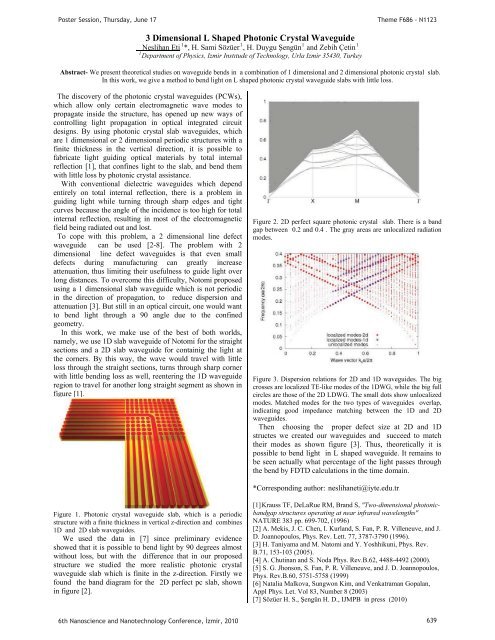
Figure 3. Dispersion relations for 2D and 1D waveguides. The big<br />
crosses are localized TE-like modes of the 1DWG, while the big full<br />
circles are those of the 2D LDWG. The small dots show unlocalized<br />
modes. Matched modes for the two types of waveguides overlap,<br />
indicating good impedance matching between the 1D and 2D<br />
waveguides.<br />
Then choosing the proper defect size at 2D and 1D<br />
structes we created our waveguides and succeed to match<br />
their modes as shown figure [3]. Thus, theoretically it is<br />
possible to bend light in L shaped waveguide. It remains to<br />
be seen actually what percentage of the light passes through<br />
the bend by FDTD calculations in the time domain.<br />
*Corresponding author: 2Tneslihaneti@iyte.edu.tr2T<br />
Figure 1. Photonic crystal waveguide slab, which is a periodic<br />
structure with a finite thickness in vertical z-direction and combines<br />
1D and 2D slab waveguides.<br />
We used the data in [7] since preliminary evidence<br />
showed that it is possible to bend light by 90 degrees almost<br />
without loss, but with the difference that in our proposed<br />
structure we studied the more realistic photonic crystal<br />
waveguide slab which is finite in the z-direction. Firstly we<br />
found the band diagram for the 2D perfect pc slab, shown<br />
in figure [2].<br />
[1]2TKrauss TF, DeLaRue RM, Brand S, "Two-dimensional photonicbandgap<br />
structures operating at near infrared wavelengths"<br />
NATURE 383 pp. 699-702, (1996)<br />
[2] A. Mekis, J. C. Chen, I. Kurland, S. Fan, P. R. Villeneuve, and J.<br />
D. Joannopoulos, Phys. Rev. Lett. 77, 3787-3790 (1996).<br />
[3] H. Taniyama and M. Natomi and Y. Yoshhikuni, Phys. Rev.<br />
B.71, 153-103 (2005).<br />
[4] A. Chutinan and S. Noda Phys. Rev.B.62, 4488-4492 (2000).<br />
[5] S. G. Jhonson, S. Fan, P. R. Villeneuve, and J. D. Joannopoulos,<br />
Phys. Rev.B.60, 5751-5758 (1999)<br />
[6] Natalia Malkova, Sungwon Kim, and Venkatraman Gopalan,<br />
Appl Phys. Let. Vol 83, Number 8 (2003)<br />
<br />
6th Nanoscience and Nanotechnology Conference, zmir, <strong>2010</strong> 639


