

Third Day Poster Session, 17 June 2010 - NanoTR-VI
Third Day Poster Session, 17 June 2010 - NanoTR-VI
Third Day Poster Session, 17 June 2010 - NanoTR-VI

You also want an ePaper? Increase the reach of your titles
YUMPU automatically turns print PDFs into web optimized ePapers that Google loves.
<strong>Poster</strong> <strong>Session</strong>, Thursday, <strong>June</strong> <strong>17</strong><br />
Theme F686 - N1123<br />
Routing Congestion Removing of Nano/CMOS FPGA circuits<br />
Hossein Hamidipour 1 , Parviz Keshavarzi 1 and Ali Naderi 1,*<br />
1 Electrical and Computer Engineering Faculty, Semnan University, Semnan, Iran<br />
Abstract CMOS Molecular (CMOL) architecture basically called hybrid nanowire/ molecular/ semiconductor circuit<br />
which incorporates the nanodevices and nanowires crossbar into the CMOS IC implementation. CMOL technology uses the<br />
advantages of nano and CMOS technology together. In this paper we have proposed a recursive method for removing the<br />
routing congestion in nano/CMOS (CMOL) FPGA circuits and route them successfully where CMOLCAD tool cannot route<br />
them without congestion. CMOL FPGA architecture, with T basic cells and a latch cell per tile, uses K basic cells (which is<br />
predefined by user), a latch cell for logic implementation and (T-K) cells for routing issue. When the circuit encountered<br />
congestion, CMOLCAD tool decreases K to route the circuits. In this proposed method, we keep and rank the placement<br />
solutions in some of the last iterations of placement algorithm, according to the cost then use them for routing the circuits<br />
with more options. If the routing on the highest priority placement solution has failed, this solution will be removed from the<br />
ranking and another placement solution will be used according to the ranking. The results of applying the proposed method<br />
on some of benchmark circuits indicate that we can route the failed routing nano/CMOS circuits without change the structure.<br />
Silicon technology continues to advance towards the end of<br />
Moores Law, predicted with the end of CMOS scaling only 1015<br />
years away. The theorical and experimental [1, 2] results indicate that<br />
the plausible alternative for current technology is hybrid<br />
semiconductor/ nanodevices circuits. This structure uses the<br />
functionality of programmable diodes (latching-switches) in crossbar<br />
structure (Fig. 1.a) beside the silicon chip. The functionality of such<br />
devices is illustrated in Fig.1.1b. CMOS Molecular (CMOL) [3]<br />
architecture basically called hybrid nanowire/ molecular/<br />
semiconductor circuit which incorporates the nanodevices and<br />
nanowire crossbar into the CMOS IC implementation. CMOL<br />
technology uses the advantages of nano and CMOS technology<br />
together.<br />
(a)<br />
proposed method routes the circuit without congestion by predefined<br />
K or we test all of the kept solutions. In this procedure the cell<br />
connectivity domain (A) is constant. In fact we use routing driven<br />
placement for nano FPGA circuits. For testing the feasibility and<br />
efficiency of the proposed method we have selected 10 circuits<br />
(MCNC benchmark and some of other circuits) that CMOLCAD tool<br />
cannot route them without congestion by predefined values of A and<br />
K. Each circuit has been implemented by original CMOLCAD and<br />
our proposed method. In original CMOLCAD, the circuits could not<br />
be routed successfully on final placement platform but the proposed<br />
method can route these failed routing circuits successfully. The<br />
results show that our method results in only 1.5% and 1% increase in<br />
area and timing cost respectively for total cost of ten circuits.<br />
Total analysis shows that the additional CPU time for running our<br />
method for ten circuits is 26.5 seconds while total time for<br />
CMOLCAD is 313 seconds. This means only 8.5% increase in CPU<br />
time for running our method.<br />
In this paper we first review the nano/CMOS hybrid circuits<br />
(CMOL) and then we discuss about their design automation and<br />
congestion. Finally we explain our method and the results.<br />
In summary the proposed method by a recursive process routes the<br />
nano/CMOS circuits which had faced congestion in CMOLCAD. It<br />
can be seen that by paying negligible additional costs, we route the<br />
failed routing circuits. This method can be added to CMOLCAD and<br />
other nano circuit CADs for removing congestion and route the<br />
circuits successfully with higher probability.<br />
(b)<br />
Figure 1: (a) Nanowire/nanodevice crossbar (b) I-V curve of a twoterminal<br />
crosspoint nanodevice-programmable diode.<br />
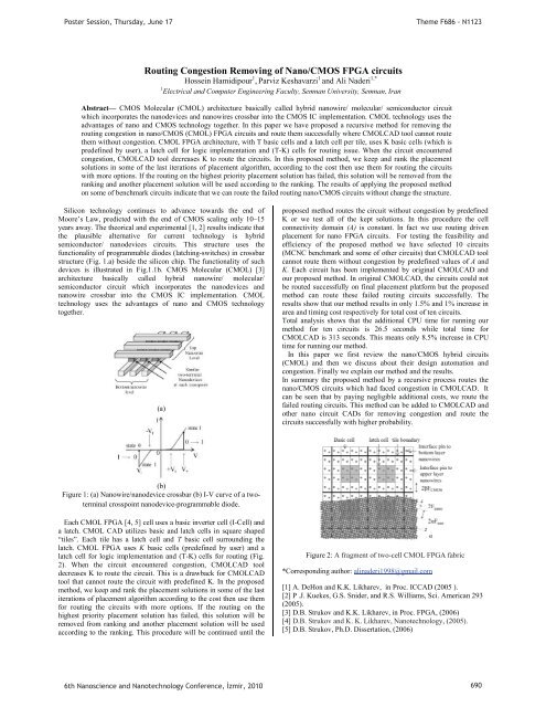
Each CMOL FPGA [4, 5] cell uses a basic inverter cell (I-Cell) and<br />
a latch. CMOL CAD utilizes basic and latch cells in square shaped<br />
tiles. Each tile has a latch cell and T basic cell surrounding the<br />
latch. CMOL FPGA uses K basic cells (predefined by user) and a<br />
latch cell for logic implementation and (T-K) cells for routing (Fig.<br />
2). When the circuit encountered congestion, CMOLCAD tool<br />
decreases K to route the circuit. This is a drawback for CMOLCAD<br />
tool that cannot route the circuit with predefined K. In the proposed<br />
method, we keep and rank the placement solutions in some of the last<br />
iterations of placement algorithm according to the cost then use them<br />
for routing the circuits with more options. If the routing on the<br />
highest priority placement solution has failed, this solution will be<br />
removed from ranking and another placement solution will be used<br />
according to the ranking. This procedure will be continued until the<br />
Figure 2: A fragment of two-cell CMOL FPGA fabric<br />
*Corresponding author: alinaderi1998@gmail.com<br />
[1] A. DeHon and K.K. Likharev, in Proc. ICCAD (2005 ).<br />
[2] P .J. Kuekes, G.S. Snider, and R.S. Williams, Sci. American 293<br />
(2005).<br />
[3] D.B. Strukov and K.K. Likharev, in Proc. FPGA, (2006)<br />
[4] D.B. Strukov and K. K. Likharev, Nanotechnology, (2005).<br />
[5] D.B. Strukov, Ph.D. Dissertation, (2006)<br />
6th Nanoscience and Nanotechnology Conference, zmir, <strong>2010</strong> 690


