

Third Day Poster Session, 17 June 2010 - NanoTR-VI
Third Day Poster Session, 17 June 2010 - NanoTR-VI
Third Day Poster Session, 17 June 2010 - NanoTR-VI

Create successful ePaper yourself
Turn your PDF publications into a flip-book with our unique Google optimized e-Paper software.
P<br />
P<br />
P<br />
P<br />
P<br />
<strong>Poster</strong> <strong>Session</strong>, Thursday, <strong>June</strong> <strong>17</strong><br />
Theme F686 - N1123<br />
Electrical and Optical Properties of Al Doped ZnO Film and Potential Applications of Gas Sensors<br />
1,2<br />
1,2<br />
1,2<br />
1,2<br />
UO. SancakogluUP<br />
P*, M. ErolP<br />
P, M. BektasP<br />
P, F. EbeoglugilP<br />
P, H. SozbilenP<br />
3P, O. Mermer 2,3P, E. Celik 1,2<br />
1<br />
PDokuz Eylul University, Department of Metallurgical and Materials Engineering, Tinaztepe Campus, 35160 Buca, Izmir-Turkey.<br />
2<br />
PDokuz Eylul University, Center for Fabrication and Application of Electronic Materials (EMUM), Tinaztepe Campus, 35160<br />
Buca, Izmir-Turkey<br />
3<br />
PEge University, Deparment of Electrical and Electronics Engineering, 35100, Bornova, Izmir-Turkey.<br />
Abstract-Undoped and Al doped semiconductor ZnO films on Si(100) and glass substrates were prepared by sol-gel technique. For this<br />
propose, transparent solutions were prepared with Zn and Al based precursors. The solutions were deposited on glass substrates using spin<br />
coating technique which decreases the film thickness up to nanoscale and gives the coating a smooth characteristic. Deposited films were dried<br />
o<br />
o<br />
at 300P PC for 10 min in order to remove hydrous and volatile content, subsequently films were heat treated at 500P PC for 5 min. to remove<br />
o<br />
organic contents and then to obtain ZnO phase structure the films were annealed at 600P PC for 1 hour in air atmosphere. Finally the surface<br />
morphologies and roughness values of the films were determined via AFM (atomic force microscopy) and profilometer, respectively. The<br />
structural and optical properties of these films have been investigated by XRD (x-ray diffractometer) and optical properties such as<br />
transmittance spectrum, optical band gap, and optical constants (refractive index, extinction coefficient, real and imaginary parts of the dielectric<br />
constant) of the films were determined.<br />
Zinc oxide (ZnO) has attracted extensive interest because<br />
of its important role in various applications, for example, gas<br />
sensor [1], varistors [2], surface acoustic wave devices [3],<br />
optical waveguides [4] as well as blue/UV light emitting<br />
devices [5]. In addition, ZnO has been considered as an<br />
excellent candidate to replace indium tin oxide (ITO) and tin<br />
oxide (SnO2) as transparent conductive electrodes in flat panel<br />
display and solar cell devices [6,7]. The advantages of zinc<br />
oxide include inexpensiveness and relative ease of<br />
lithography. However, the electrical conductivity of un-doped<br />
zinc oxide is not high enough for practical application. Further<br />
reduction of resistivity of zinc oxide can be achieved either by<br />
doping group III elements such as B, Al, In and Ga to replace<br />
zinc atoms [8] or group IV elements, F, to substitute oxygen<br />
atoms [9].<br />
The structural and morphological properties of<br />
semiconductor oxides have a substantial effect on their optical,<br />
electrical and gas sensing properties. The controlledparticle<br />
size and morphology facilitate the desired characteristics in<br />
the materials. Several simplewet chemical routes like sol–gel,<br />
co-precipitation and Pechini route have been adapted to form<br />
nanostructures [10].<br />
specific acid-alcohol medium to remove the contaminations<br />
and prepare the surface for sol-gel coating. The films were<br />
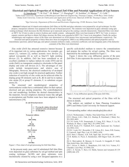
deposited by the technique detailed in Figure 1.<br />
Figure 2 shows the x-ray diffraction spectra of the pure<br />
ZnO film. It also represents the success of the coating process.<br />
Figure 2. X-ray diffraction spectra of the pure ZnO film.<br />
The structural and optical properties of the films will be<br />
shown in details. b)<br />
The authors are indebted to State Planning Foundation<br />
(DPT) and Dokuz Eylul University for financial support.<br />
*Corresponding author: orkut.sancakoglu@deu.edu.tr<br />
Figure 1. Flow chart of sol-gel processing for ZnO thin films.<br />
In the present study; pure, and Al substituted ZnOR Rthin films<br />
were deposited on glass substrates by sol-gel method and spin<br />
coating technique. Si(100) and glass substrates were<br />
mechanically cleaned by using a new designed apparatus in a<br />
[1] K.S. Weibenrieder, J. Muller, Thin Solid Films 30 (1997) 30.<br />
[2] E. Olsson, L.K.L. Falk, G.L. Dunlop, R. Osterlund, J. Mater. Sci.<br />
20 (1985) 4091.<br />
[3] C.R. Gorla, N.W. Emanetoglu, S. Liang, W.E. Mayo, Y. Lu, M.<br />
Wraback, H. Shen, J. Appl. Phys. 85 (1999) 2595.<br />
[4] M.H. Koch, P.Y. Timbrell, R.N. Lamb, Semicond. Sci. Technol.<br />
10 (1995) 1523.<br />
[5] D.C. Look, D.C. Reynolds, C.W. Litton, R.L. Jones, D.B. Easton,<br />
G. Cantwell, Appl. Phys. Lett. 81 (2002) 1830.<br />
[6] G. Hass, J. Heaney, A.R. Toft, Appl. Opt. 18 (1975) 1488.<br />
[7] R. Barber, G. Pryor, E. Reinheimer, SID Digest Tech. 28 (1997)<br />
18.<br />
[8] G. Sberveglieri, B. Benussi, G. Coccoli, S. Groppelli, P. Nelli,<br />
Thin Solid Films 186 (1990) 349.<br />
[9] C. Grivas, S. Mailis, L. Boutsikaris, D.S. Gill, N.A. Vainos, P.J.<br />
Chandler, Laser Phys. 8 (1998) 326.<br />
[10] C. S. Navale, V. Ravi, I.S. Mulla, Sensors and Actuators B 139<br />
(2009) 466–470<br />
6th Nanoscience and Nanotechnology Conference, zmir, <strong>2010</strong> 702


