

Third Day Poster Session, 17 June 2010 - NanoTR-VI
Third Day Poster Session, 17 June 2010 - NanoTR-VI
Third Day Poster Session, 17 June 2010 - NanoTR-VI

You also want an ePaper? Increase the reach of your titles
YUMPU automatically turns print PDFs into web optimized ePapers that Google loves.
<strong>Poster</strong> <strong>Session</strong>, Thursday, <strong>June</strong> <strong>17</strong><br />
Theme F686 - N1123<br />
Epitaxial Graphene Synthesis on Silicon Carbide Substrate<br />
Hüsnü Aslan 1 , 1 ,NihanÖzkan 2 ,and Ahmet Oral 1<br />
1 Faculty of Engineering & Natural Sciences University, Istanbul, 34956, Turkey<br />
2 Department of Physics Engineering, Istanbul Technical University, 34469, Turkey<br />
Abstract – Large scale single layer epitaxial graphene is going to be produced in the ultrahigh vacuum chamber and<br />
characterized by Atomic Force Microscope and Low Energy Electron Diffraction.<br />
Graphene, one atomic thick layer form of graphite,<br />
is composed of hexagonally arranged carbon atoms and<br />
the layers between two graphene sheets are bonded by<br />
weak van der Waals interaction. Its unique electrical<br />
and mechanical properties have recently made it popular<br />
in both science and technology.<br />
Graphene could be produced by using several methods<br />
both chemically and mechanically. The most popular<br />
and the easiest method is called mechanical<br />
exfoliation[1]. However, by using this method one can<br />
produce small-area graphene layer. In order to obtain<br />
large scale graphene, the method called epitaxial growth<br />
on SiC or CVD can be used. This method includes two<br />
steps. For the first step, SiC has to be etched by<br />
hydrogen gas in order to prepare suitable SiC surface<br />
for epitaxial growth. In this process, cleaned SiC<br />
samples are annealed in a vacuum chamber with %5 H 2<br />
and %95 Ar gas flow. For the second step, SiC chip is<br />
heated in ultrahigh vacuum to temperatures between<br />
1000-1500°C in order to sublimate Si [2,3].<br />
In this work, we are planning to produce monolayer<br />
graphene on commercially available 4H-SiC(0001)<br />
sample. The growth process is going to be performed in<br />
an ultrahigh vacuum chamber equipped with e-beam<br />
heater and graphene layers are going to be characterized<br />
by Low Energy Electron Diffraction (LEED). In<br />
addition to this, thickness of this graphene layer is going<br />
to be measured by Atomic Force Microscope.<br />
ers<br />
107T720, 107T892 & 108T930 and NanoMagnetics<br />
Instruments Ltd.<br />
[1] Geim, A-K., and Novoselov, K-S.The rise of graphene,<br />
Nature Materials, 6, 183-191(2007).<br />
[2]Hass, J., De Heer, W.A., and Conrad, E.H. The growth and<br />
morphology of epitaxial multilayer graphene, Journal of<br />
physics: Condensed Matter, 20, 323202 (2008).<br />
[3]Ramachandran V., Brady, M.F., Smith, A.R., Feenstra,<br />
R.M., and Greve, D.W. Preparation of atomically flat surfaces<br />
on silicon carbide using hydrogen etching, Journal of<br />
Electronic Materials, 27, 308-312, (1998)<br />
.<br />
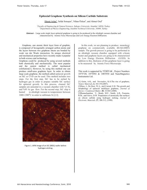
Figure 1. AFM image of an SiC (0001) wafer before<br />
hydrogen etching.<br />
6th Nanoscience and Nanotechnology Conference, zmir, <strong>2010</strong> 666


