

Third Day Poster Session, 17 June 2010 - NanoTR-VI
Third Day Poster Session, 17 June 2010 - NanoTR-VI
Third Day Poster Session, 17 June 2010 - NanoTR-VI

You also want an ePaper? Increase the reach of your titles
YUMPU automatically turns print PDFs into web optimized ePapers that Google loves.
P<br />
P mP<br />
P vs.<br />
P =<br />
P,P<br />
P (1)<br />
P and<br />
<strong>Poster</strong> <strong>Session</strong>, Thursday, <strong>June</strong> <strong>17</strong><br />
Theme F686 - N1123<br />
Influence of Annealing Conditions on Optical Properties of ZnO Thin Films<br />
1<br />
1<br />
1<br />
1<br />
1<br />
1<br />
UDerya BaharUP P*, Göknil BabürP P, Sinan DikenP P, Tuba Aye TermeliP P, Banu ErdoanP P, Sava SönmezoluP<br />
Pand Güven ÇankayaP<br />
1<br />
PDepartment of Physics, Faculty of Arts and Science, Gaziosmanpaa University, Tokat 60250, Turkey<br />
Abstract-ZnO thin films were deposited on soda lime glass substrates by sol–gel spin-coating technique. The optical properties of ZnO thin films<br />
are investigated for different annealing temperatures. The optical band gaps of thin film are found to vary with annealing temperatures. The<br />
obtained films are also transparent in the UV- visible region<br />
1<br />
Zinc oxide (ZnO) as a wide-band-gap semiconductor has<br />
attracted much attention in current semiconductor research,<br />
due to its superior optical properties. In addition, ZnO is a<br />
versatile semiconductor material, which has attracted attention<br />
for its wide range of applications, such as thin films, solar<br />
cells, luminescent, electrical and acoustic devices and<br />
chemical sensors [1-2].<br />
In this paper, we report the investigation of ZnO thin films<br />
prepared by sol-gel spin coating process using zinc acetate<br />
(ZnAc). The optical characterization is investigated for<br />
different annealing temperatures using Perkin Elmer Lambda<br />
35 UV-<strong>VI</strong>S Spectrometer at room temperature.<br />
Transmittance (%)<br />
100<br />
80<br />
60<br />
40<br />
20<br />
0<br />
200 400 600 800 1000 1200<br />
Wavelenght (nm)<br />
200 C 0<br />
300 C 0<br />
400 C 0<br />
500 C 0<br />
Figure 1. UV–<strong>VI</strong>S spectra of the ZnO thin film for various<br />
temperatures.<br />
In order to prepare a ZnO solution, first, 3.35gr zinc acetate<br />
(Zn(CHR3RCOO)R2R·2HR2RO, Merck), used as a precursor, was<br />
dissolved in 50 ml ethanol [CR2RHR6RO, Merck] and stirred for 5<br />
0<br />
min at 60 P PC in a magnetic mixture. Then, 5 ml glacial acetic<br />
acide [CR2RHR4ROR2R, Merck] and 1.5 ml hydrochloride acid (HCl,<br />
Merck) were added in the solution, and the final solution was<br />
subjected to the magnetic mixture for 2 h. Here, glacial acetic<br />
acid and hydrochloride acid were used as an inhibitor to slow<br />
down the zinc acetate fast hydrolysis. Prior to the coating<br />
process, the glass was washed with water, ultrasonically<br />
cleaned in ethanol for 20 min, and in acetone for 20 min,<br />
respectively. The deposition was carried out at a spinning<br />
speed of 3000 rpm for 30 s. The spin coating procedure was<br />
0 0 0<br />
continuously repeated five times at 200P PC, 300P PC, 400P PC and<br />
0<br />
500P PC annealing temperatures on glass substrate.<br />
Fig. 1 shows the UV–<strong>VI</strong>S spectra ZnO thin films for<br />
different annealing temperatures in wavelength range 300–<br />
1100nm. The transmission of the thin films of zinc oxide<br />
decreases with the increase in annealing temperature. This can<br />
be linked with the increase in the grain size, and indicating its<br />
high surface roughness and inhomogeneity [3].<br />
(h v) 2 (eV/m) 2<br />
20<br />
16<br />
12<br />
8<br />
4<br />
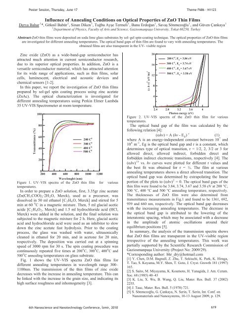
200 C 0 , E g<br />
= 3.84 eV<br />
300 C 0 , E g<br />
= 3.74 eV<br />
400 C 0 , E g<br />
= 3.67 eV<br />
500 C 0 , E g = 3.58 eV<br />
0<br />
2.4 2.8 3.2 3.6 4<br />
Photon energy (eV)<br />
Figure 2. UV–<strong>VI</strong>S spectra of the ZnO thin film for various<br />
temperatures.<br />
The optical band gap of the film was calculated by the<br />
following relation [4]:<br />
(hv) = A (hv - ERgR) P<br />
7<br />
where A is an energy-independent constant between 10P<br />
8 -1<br />
10P<br />
P, Eg is the optical band gap and r is a constant, which<br />
determines type of optical transition, r = 1/2, 2, 3/2 or 3 for<br />
allowed direct, allowed indirect, forbidden direct and<br />
forbidden indirect electronic transitions, respectively [4]. The<br />
1/r<br />
r<br />
(hv)P hv curves were plotted for different r values and<br />
the best fit was obtained for r = ½. The film at various<br />
annealing temperatures shows a direct allowed transition. The<br />
optical band gap was determined by extrapolating the linear<br />
2<br />
portion of the plots to (hv)P 0. The optical band gaps of the<br />
thin film were found to be 3.84, 3.74, 3.67 and 3.58 eV at 200 °C,<br />
300 °C, 400 °C and 500 °C annealing temperature, respectively.<br />
The thicknesses of ZnO film were also determined from<br />
transmittance measurements in Fig.1 and found to be 1361, 692,<br />
939 and 660 nm, respectively. The optical band gap decreases<br />
with the increasing annealing temperatures. The decrease in<br />
the optical band gap is attributed to the lowering of the<br />
interatomic spacing, which may be associated with a decrease<br />
in the amplitude of atomic oscillations around their<br />
equilibrium positions [5].<br />
In summary, the analysis of the transmission spectra shows<br />
that ZnO thin films are transparent in the UV-visible region<br />
irrespective of the annealing temperatures. This work was<br />
partially supported by the Scientific Research Commission of<br />
Gaziosmanpaa University (Project No: 2009/29).<br />
*Corresponding author: HTbhr_dry@hotmail.comT<br />
[1] Y. Chen, D.M. Bagnall, Z. Zhu, T. Sekiuchi, K. Park, K. Hiraga,<br />
T. Tao, S. Koyama, M.Y. Shen, T. Goto, J. Cryst. Growth 181 (1997)<br />
165.<br />
[2] S. Saito, M. Miyayama, K. Koumoto, H. Yanagida, J. Am. Ceram.<br />
Soc. 68 (1985) 40–43<br />
[3] K. Liu, X. Wu, B. Wang, Q. Liu, Mater. Res. Bull. 37 (2002)<br />
2255.<br />
[4] J. Tauc, Mater. Res. Bull. 5 (1970) 721.<br />
[5] S. Sönmezolu, G. Çankaya,P PN. Serin, T. Serin, Int. Conf. on<br />
Nanomaterials and Nanosystems, 10-13 August 2009, p. 129.<br />
6th Nanoscience and Nanotechnology Conference, zmir, <strong>2010</strong> 619


