

Third Day Poster Session, 17 June 2010 - NanoTR-VI
Third Day Poster Session, 17 June 2010 - NanoTR-VI
Third Day Poster Session, 17 June 2010 - NanoTR-VI

You also want an ePaper? Increase the reach of your titles
YUMPU automatically turns print PDFs into web optimized ePapers that Google loves.
P<br />
P and<br />
<strong>Poster</strong> <strong>Session</strong>, Thursday, <strong>June</strong> <strong>17</strong><br />
Theme F686 - N1123<br />
Photon Scanning Tunneling Microscopy System for Observing Optical Excitations at Nanoscale<br />
Tunnel Junctions<br />
1<br />
1<br />
1<br />
Tansu ErsoyP P, Mehmet Selman TamerP<br />
UOuzhan GürlüUP P*<br />
1<br />
Pstanbul Technical University, Department of Physics, Maslak, 34469, stanbul, Turkey<br />
Abstract-We are developing an optical system which is capable of collecting the photons emitted from the tunnel junction of a scanning<br />
tunneling microscope. These systems allow mapping the photon emission from a surface with sub nanometer spatial resolution. Electronic and<br />
optical properties of nanostructures like quantum dots or quantum wires will be studied by this system.<br />
Images with atomic resolution of semiconductor and metal<br />
surfaces can be obtained using scanning tunneling microscopy<br />
(STM) [1]. Moreover optical and electronic properties of these<br />
surfaces can be examined by STM at nanoscale [2]. The<br />
tunneling current between the tip and the surface can excite<br />
optical transitions on the surface [3]. This is called<br />
electroluminescence due to inelastic tunneling. STM-light<br />
emission experiment is a recently emerging and very useful<br />
technique for investigating optical properties of surfaces with<br />
nanometer resolution [4].<br />
Nanostructures have different characteristics from bulk<br />
materials. As the size of the materials approach to nanoscale,<br />
quantum effects appear, which is very important for device<br />
applications [5]. If a semiconductor crystal becomes very<br />
small, motion of the charge carriers is restricted. This<br />
phenomenon is known as quantum confinement. This results<br />
in sharp electronic states in these structures. In order to<br />
understand quantum effects there are numerous studies for<br />
developing nanostructures and methods for investigating their<br />
electronic and optical properties [4,5,6].<br />
Metals also behave unconventionally physical properties at<br />
nano scale. For instance Ag films coated on glass or mica has<br />
a rough structure due to which the surface plasmon polaritons<br />
are confined. These effects the optical properties of the films<br />
greatly like giving the film unexpected color. Using the<br />
photon scanning microscope one can study the local electrooptical<br />
properties [7] of these films and their interaction with<br />
adsorbates.<br />
most efficient way [10] and they have to be spectroscopically.<br />
analyzed. Thus, electroluminescence spectroscopy at<br />
nanoscale can be performed.<br />
Figure 2. In inelastic tunneling, electrons that tunnel from the tip to<br />
the surface lose some of their energy. Photons are generated in this<br />
process. Energy lost due to excitations can be observed by<br />
conductivity measurements. They appear as peaks in the second<br />
derivative of the tunneling current with respect to sample bias [9].<br />
Figure 3. A simple representation of photon STM setup.<br />
First we are planning to investigate optical properties of<br />
metal surfaces like vacuum evaporated rough Au or Ag films<br />
on glass. Later on we will investigate core/shell quantum dots<br />
like CdSe/ZnS. Optical behavior of QDs on gold surfaces will<br />
be observed by STM induced light emission technique.<br />
Depending on structures and positions of QDs on gold surface<br />
we are expecting variations in their optical behaviors.<br />
Moreover, we will investigate the results of the interactions of<br />
QDs with various surfaces and with their environments.<br />
*Corresponding author: HTgurlu@itu.edu.trTH<br />
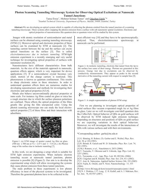
Figure.1. (a) STM image of sputter coated Ag film on glass.<br />
(500 nm x 500 nm at Vs = 2.0 V and I = 5.0 nA.). (b) Photon<br />
map of the surface due to inelastic tunneling [7].<br />
In this work, we are designing a setup which is suitable for<br />
STM light emission experiments. When inelastic electron<br />
tunneling occurs at nanoscale tunnel junctions, photon<br />
emission is possible [8] (Figure.2). Our aim is to develop the<br />
experimental setup which will allow investigating the systems<br />
that cause photon emission from these tunnel junctions.<br />
The main problem in these experiments is low photon<br />
efficiency in most of the physical systems to be investigated.<br />
Therefore the generated photons have to be collected in the<br />
[1] G. Binning, H. Rohrer, Ch. Gerber and E. Weibel, Phys. Rev.<br />
Lett. 50, p 120 (1983).<br />
[2] R. Berndt, R. Gaisch and W. D. Schneider, Phys. Rev. Lett. 74,<br />
102 (1995).<br />
[3] M,J. Romero, et al., Nanoletters 6, 2833 (2006).<br />
[4] T. Tsuruoka, Y. Ohizumi and S. Ushioda, App. Phys. Lett. 82,<br />
3257 (2003).<br />
[5] L. Turyanska, et al., App. Phys. Lett. 89, 092106, (2006)<br />
[6] R. Cingolani and R. Rinaldi, Phys. Stat. Sol. 234, 411 (2002).<br />
[7] T. Arai, K. Nakayama, Applied Surface Science 246, 193 (2005)<br />
[8] D. Fujita, K. Onishi, and N. Niori, Nanotechnology 15, 355<br />
(2004).<br />
[9] http://www.fkf.mpg.de/kern/research/nanooptics/pstm.1.html<br />
[10] N. J. Watkins, J. P. Long, Z. H. Kafafi, and A. J. Makinen, Rev.<br />
Sci. Inst. 78, 053707 (2007).<br />
6th Nanoscience and Nanotechnology Conference, zmir, <strong>2010</strong> 623


