

Third Day Poster Session, 17 June 2010 - NanoTR-VI
Third Day Poster Session, 17 June 2010 - NanoTR-VI
Third Day Poster Session, 17 June 2010 - NanoTR-VI

You also want an ePaper? Increase the reach of your titles
YUMPU automatically turns print PDFs into web optimized ePapers that Google loves.
P<br />
P and<br />
770 772 774 776 778 780 782 784 786 788 790<br />
<strong>Poster</strong> <strong>Session</strong>, Thursday, <strong>June</strong> <strong>17</strong><br />
Theme F686 - N1123<br />
Characterization of a Multilayer GaAs/AlGaAs Broadband Quantum Well Infrared Photodetectors<br />
1<br />
1<br />
1<br />
1<br />
1<br />
UHülya KuruUP P*, Burcu ArpapayP P, Bülent ArkanP P, Bülent AslanP Uur SerincanP<br />
1<br />
PDepartment of Physics, Anadolu University, Eskiehir 26470, Turkey<br />
Abstract-In this study, we report on the investigation of a multilayer GaAs/AlGaAs quantum well infrared photodetector designed for 8-12 m<br />
spectral range detection. Fabricated devices were characterized by performing various methods of measurements: current-voltage,<br />
photoluminescence and photoresponse as a function of applied bias.<br />
After developing the ability to grow multilayer<br />
semiconductor quantum structures, GaAs/AlGaAs multiple<br />
quantum wells (MQWs) have been intensively investigated<br />
because of their potential applications in advanced optoelectronic<br />
devices [1]. These studies resulted in a continuous<br />
improvement of the performances and the appearance of novel<br />
devices. In particular, infrared detectors based on intersubband<br />
transitions in GaAs/AlGaAs MQW structures exhibit many<br />
advantages over the conventional band-to-band HgCdTe<br />
detectors, and represent an interesting alternative for the<br />
detection of the mid- and far-infrared regions (i.e. wavelengths<br />
longer than 3μm) [1,2].<br />
The sample used in this study was grown by molecular beam<br />
epitaxy (MBE) on (100) GaAs substrate. It consists of 10<br />
periods of the following symmetric structure (from substrate<br />
to top): 40 nm of AlGaAs (20% Al) barrier, 6 nm GaAs QW,<br />
20 nm AlGaAs (20% Al), 10 nm graded AlGaAs (from 20%<br />
to 25% Al), 10 nm AlGaAs (25% Al), 5 nm GaAs QW. This<br />
10 repeat structure is sandwiched between a 6 nm GaAs QW<br />
and thick doped contact layers. The central parts of the wells<br />
are Si-doped to have the active carriers in the structures. The<br />
top and bottom GaAs contact layers are 400 nm and 700 nm,<br />
18 2<br />
respectively and doped with 1×10P<br />
P cmP P. Mesas were defined<br />
by wet chemical etching and top and bottom contacts were<br />
made by depositing Ge/Au/Ni/Au followed by annealing.<br />
Different size square devices (400 m, 600 m, 800 m, 1000<br />
m and 1500 m) having a ring top contact were fabricated to<br />
test the uniformity of the wafer and the quality of the<br />
fabrication. For the photoresponse (PR) measurements, sample<br />
was mounted in a liquid nitrogen cooled dewar with ZnSe<br />
window. A Bruker Equinox55 Fourier transform infrared<br />
spectrometer with a globar source was used. A 7 mW HeNe<br />
laser (632.8nm) was used as an excitation source in<br />
photoluminescence experiments. For optical measurements,<br />
devices were illuminated through the top opening. All<br />
measurements were performed at a cold head temperature of<br />
80 K.<br />
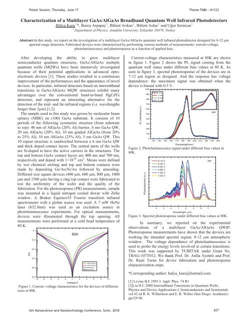
I(A)<br />
0.1<br />
0.01<br />
1E-3<br />
1E-4<br />
1E-5<br />
80K<br />
1500*1500m 2<br />
1000*1000m 2<br />
800*800m 2<br />
600*600m 2<br />
1E-6<br />
-10 -8 -6 -4 -2 0 2 4 6 8 10<br />
Voltage(V)<br />
Figure 1. Current–voltage characteristics for the devices of different<br />
sizes at 80K.<br />
Current-voltage characteristics measured at 80K are shown<br />
in figure 1. Figure 2 shows the PL signal coming from the<br />
quantum well states under different bias values at 80 K. As<br />
seen in figure 3, spectral photoresponse of the devices are in<br />
7-12 m region as designed. And the response has voltage<br />
dependence: the maximum signal was obtained when the<br />
device is biased with 0.5 V.<br />
PL Intensity(a.u.)<br />
1000<br />
900<br />
800<br />
700<br />
600<br />
500<br />
400<br />
300<br />
200<br />
100<br />
0<br />
0 volt<br />
1 volt<br />
2 volt<br />
3 volt<br />
730 740 750 760 770 780 790 800 810 820 830 840<br />
Wavelength(nm)<br />
Figure 2. Photoluminescence signal under different bias values at<br />
80K.<br />
Photoresponse (a.u.)<br />
0.15 V<br />
0.30 V<br />
0.50 V<br />
0.80 V<br />
1.00 V<br />
1.30 V<br />
4 5 6 7 8 9 10 11<br />
Wavelength (m)<br />
Figure 3. Spectral photoresponse under different bias values at 80K.<br />
In summary, we reported on the experimental<br />
observations of a multilayer GaAs/AlGaAs QWIP.<br />
Photoresponse measurements have shown that the devices are<br />
working the intended spectral region: 8-12 m atmospheric<br />
window. The voltage dependence of photoluminescence is<br />
used to probe the energy levels involved in certain transitions.<br />
This work was supported by TUBITAK under Grant No.<br />
TBAG-107T012. We thank Prof. Dr. Atilla Aydnl and Prof.<br />
Dr. Rait Turan for device fabrication and photoresponse<br />
characterization steps.<br />
*Corresponding author: hulya_kuru@hotmail.com<br />
[1] Levine B.F.1993 J. Appl. Phys. 74 R1<br />
[2]Liu H.C.2000 Intersubband Transitions in Quantum Wells:<br />
Physics and Device Applications I, Semiconductors and Semimetals<br />
vol 62 ed R. K. Willardson and E. R. Weber (San Diego: Academic)<br />
pp129-96<br />
80K<br />
80K<br />
6th Nanoscience and Nanotechnology Conference, zmir, <strong>2010</strong> 627


