

Third Day Poster Session, 17 June 2010 - NanoTR-VI
Third Day Poster Session, 17 June 2010 - NanoTR-VI
Third Day Poster Session, 17 June 2010 - NanoTR-VI

You also want an ePaper? Increase the reach of your titles
YUMPU automatically turns print PDFs into web optimized ePapers that Google loves.
P<br />
P mBar.<br />
P and<br />
<strong>Poster</strong> <strong>Session</strong>, Thursday, <strong>June</strong> <strong>17</strong><br />
Theme F686 - N1123<br />
Construction of a Combined Non-Contact Atomic Force Microscope & Scanning Tunnelling<br />
Microscope (nc-AFM/STM)<br />
1<br />
1<br />
1<br />
1<br />
UDerya GemiciUP P*, Hüsnü AslanP P, Özhan ÜnverdiP Ahmet OralP<br />
1<br />
PFaculty of Engineering & Natural Sciences, Sabancı University, Istanbul, 34956, Turkey<br />
Abstract-A combined non-contact Atomic Force Microscope (nc-AFM) & Scanning Tunnelling Microscope (STM) operating in Ultra<br />
High Vacuum(UHV) has been designed and constructed. The nc-AFM uses a fiber interferometer and Digiatl Phase Locked Loop for high<br />
resolution detection of cantilever displacements.<br />
In the early 1980's two IBM scientists, Binnig & Rohrer,<br />
developed a new technique for studying surface structure<br />
at atomic scale - Scanning Tunnelling Microscopy(STM).<br />
This invention was quickly followed by the development<br />
of a whole family of related techniques called Scanning<br />
Probe Microscopy (SPM). The most important SPM<br />
method is the Atomic Force Microscopy (AFM) where the<br />
tip-sample forces are measured to obtain topography of the<br />
sample even at the atomic scale. The inventions of STM<br />
and AFM revolutionised the surface science, helping<br />
scientist to resolve the atomic structure of surfaces in real<br />
space.<br />
In this work, we have designed and constructed a<br />
combined non-contact Atomic Force Microscope (nc-<br />
AFM) & Scanning Tunnelling Microscope (STM) based<br />
on fiber interferometer for the imaging surfaces ranging<br />
from non-conducting to conducting and from hard to soft<br />
and delicate samples in Ultra High Vacuum(UHV). The<br />
design is based on our previous work [3,4] with substantial<br />
improvement in vibration isolation and ease of assembly.<br />
UHV by imaging Gold evaporated on glass. STM images<br />
of this specimen is given in Figure 3.<br />
Figure 2. Optical Microscope images of home-made tungsten tips<br />
have been used for the experiment<br />
Figure 3. The STM image of of gold surface at UHV,<br />
-11<br />
p < 3×10P IRT R= 0.3 nA & VRBiasR = 1 V<br />
This work is supported by TÜBTAK , Project Number<br />
108T001, Ministry of Industry & Commerce, Project<br />
Number 409.STZ.2009-1 and NanoMagnetics Instruments<br />
Ltd.<br />
*Corresponding author: deryagemici@sabanciuniv.edu<br />
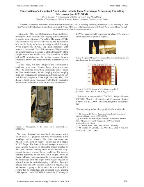
Figure 1. Photograph of the home made combined nc-<br />
AFM/STM.<br />
We have designed the combined microscope using<br />
Solidworks CAD program, the parts are machined at the<br />
workhops around Ankara. The final assembled nc-<br />
AFM/STM is shown in Figure 1 is mounted on a special<br />
8’’ CF flange. The base of the microscope is suspended<br />
using springs mounted on adjustable collars attached to<br />
four posts. In order to damp the external vibrations eddycurrent<br />
damping is used. Twenty eight SmCo magnets<br />
attached separately to the posts on a magnet holder as<br />
shown in Figure 1 are surrounded by copper plates fixed to<br />
the microscope base, the height of the magnet ring can be<br />
adjusted to set the desired damping coefficient. Tungsten<br />
tips are etched in KOH solution as shown in Figure 2. The<br />
microscope is going to be mounted in a separate UHV<br />
system, but the initial tests are performed in our existing<br />
UHV system. Nc-AFM/STM is tested for STM only in<br />
[1] G. Binning, H. Rohrer ‘Scanning Tunnelling Microscopy’,<br />
Helvetica Physica Acta, 55,726 (1982)<br />
[2 ] S.Morita,R.Wiesendanger, E.Meyer ‘Noncontact Atomic<br />
Force Microscopy’ pg 11-76 principle of NC AFM and<br />
semiconductor surfaces<br />
[3] M. Atabak, PhD Thesis, 2007, Bilkent University<br />
[4] M. Atabak, Ö. Ünverdi, H.Ö. Özer & A. Oral, J. Vac. Sci.<br />
Technol. B 27, 1001 (2009)<br />
6th Nanoscience and Nanotechnology Conference, zmir, <strong>2010</strong> 667


