

Third Day Poster Session, 17 June 2010 - NanoTR-VI
Third Day Poster Session, 17 June 2010 - NanoTR-VI
Third Day Poster Session, 17 June 2010 - NanoTR-VI

Create successful ePaper yourself
Turn your PDF publications into a flip-book with our unique Google optimized e-Paper software.
<strong>Poster</strong> <strong>Session</strong>, Thursday, <strong>June</strong> <strong>17</strong><br />
Theme F686 - N1123<br />
Physical properties of nanostructure thin films of fluorine-doped indium oxide prepared by spray<br />
pyrolysis technique<br />
S.M.Rozati, Z.Bargbidi<br />
Depatment of physics, University of Guilan, Rasht 41335, Iran<br />
Email: smrozati@guilan.ac.ir<br />
Abstract- In this research, indium oxide nanostructure undoped and doped with F were prepared on glass substrates using spray<br />
pyrolysis technique. Various parameters such as dopant concentration, deposition temperatures, amount of indium oxide powder were<br />
discussed. Structural properties of these films were investigated by XRD & SEM. Electrical and optical properties have been studied<br />
by Hall Effect and UV-Visible spectrophotometer respectively. The thickness of the films is determined by PUMA software. The<br />
variation in refractive index, extension coefficient and band gap of these films also were investigated.<br />
Transparent conducting oxide such as In 2 O 3 :F (IFO)<br />
because of their high optical transparency in the visible<br />
region, good electrical conductivity are important. There are<br />
many applications for transparent conductive oxide ( TCO)<br />
films such as solar cells, liquid crystal display, and gas<br />
sensors[1].<br />
TCO films have been prepared by various deposition<br />
techniques such as vacuum evaporation, sputtering, spray<br />
pyrolysis, sol gel, etc [2-4].<br />
In this research, IFO thin films were prepared on glass<br />
substrates using spray pyrolysis technique. In 2 O 3 :F thin films<br />
were prepared by spraying a water solution containing<br />
indium chloride (0.2gr InCl 3 ) and NH 4 F used as dopant onto<br />
glass substrates heated at different substrate temperatures.<br />
Deposition of parameters conclude: distance between the<br />
spray nozzle an substrates 25 cm, the carrier gas using<br />
filtered compressed air, the spray rate 19 lit/min, volume of<br />
solution is 40 ml.<br />
All the above mentioned parameters were kept constant and<br />
only the concentration of NH 4 F (0-15wt%) and substrate<br />
temperature (400-600 ° C) were changed.<br />
In this work we first optimize the concentration of F wt%<br />
using electrical resistivity and optical transparency and<br />
secondly focused on the effect of substrate temperature on<br />
structural, electrical, optical properties of the samples with a<br />
constant fluorine concentration of 2wt%.<br />
Concentration of F in these films have been varied from 0-<br />
15wt%. as a result, the resistivity decreased quickly with<br />
increasing F concentration reaching a minimum of<br />
=1.35x10 -3 cm for an F concentration of 1wt%. For higher<br />
dopant content, the resistivity increased. The higher<br />
transmittance observed in the films for 2wt% of F doped.<br />
Since we were looking for a layer with both high transparent<br />
and good resistevity, we used figure of merit (FOM). Thus<br />
the optimized layer with 2wt% of F concentration was<br />
selected according to the most FOM [5].<br />
The X-ray diffraction result of IFO films in various<br />
concentration are shown that, films are polycrystalline and<br />
crystallize in a cubic structure with preferential orientation<br />
along (222) and (400). Note also that no characteristic peaks<br />
of impurity and dopant phases have been observed.<br />
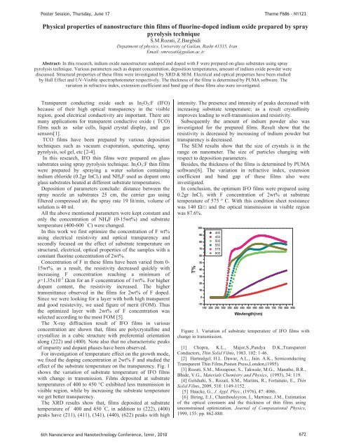
For investigation of temperature effect on the growth mode,<br />
we fixed the doping concentration at 2wt% F and studied the<br />
effect of the substrate temperature on the transparency. Fig. 1<br />
shows the variation of substrate temperature of IFO films<br />
with change in transmission. Films deposited at substrate<br />
temperatures of 400 to 450 °C exhibited less transmission in<br />
visible region, while by increasing the substrate temperature<br />
we get better transparency.<br />
The XRD results show that, films deposited at substrate<br />
temperature of 400 and 450 ° C, in addition to (222), (400)<br />
peaks have (211), (411), (341), (440), (622) peaks with high<br />
intensity. The presence and intensity of peaks decreased with<br />
increasing substrate temperature; as a result crystallinity<br />
improves leading to well-transmission and resistivity.<br />
Subsequently the amount of indium powder also was<br />
investigated for the prepared films. Result show that the<br />
resistivity is decreased by increasing of indium powder but<br />
transparency is decreased.<br />
The SEM results show that the size of crystals is in the<br />
range on nanometer. The size of particles changing with<br />
respect to deposition parameters.<br />
Besides, the thickness of the films is determined by PUMA<br />
software[6]. The variation in refractive index, extension<br />
coefficient and band gap of these films also were<br />
investigated.<br />
In conclusion, the optimum IFO films were prepared using<br />
0.2gr InCl 3 with F concentration of 2wt% at substrate<br />
temperature of 575 ° C. With this condition sheet resistance<br />
was 140 / and the optical transmission in visible region<br />
was 87.6%.<br />
T%<br />
100<br />
90<br />
80<br />
70<br />
60<br />
50<br />
40<br />
30<br />
20<br />
10<br />
0<br />
400<br />
450<br />
500<br />
550<br />
575<br />
600<br />
-10<br />
150 200 250 300 350 400 450 500 550 600 650 700 750 800 850<br />
Wavlength(nm)<br />
Figure 1. Variation of substrate temperature of IFO films with<br />
change in transmission.<br />
[1] Chopra, K.L., Major,S.,Pandya D.K.,Transparent<br />
Conductors, Thin Solid Films, 1983. 102: 1-46.<br />
[2] Hartnalgel, H.L. Dawar, A.L., Jain. A.K., Semiconducting<br />
Transparent Thin Films,Paston Press,London,(1995).<br />
[3] Rozati, S.M., Mirzapour, S., Takwale, M.G., Marathe, B.R.,<br />
Bhide, V.G., Materials Chemistry and Physics, (1993), 34: 119.<br />
[4] Golshahi, S., Rozati, S.M., Martins, R., Fortunato, E., Thin<br />
Solid Films, 2009, 518: 1149-1152.<br />
[5] Haacke, G., J. Appl. Phys., (1976), 47: 4086.<br />
[6] Biring, E.J., Chambouleyron, I., Martinez, J.M., Estimation<br />
of the optical constants and the thickness of thin films using<br />
unconstrained optimization, Journal of Computational Physics,<br />
1999, 155: pp. 862-880.<br />
6th Nanoscience and Nanotechnology Conference, zmir, <strong>2010</strong> 672


