

Third Day Poster Session, 17 June 2010 - NanoTR-VI
Third Day Poster Session, 17 June 2010 - NanoTR-VI
Third Day Poster Session, 17 June 2010 - NanoTR-VI

You also want an ePaper? Increase the reach of your titles
YUMPU automatically turns print PDFs into web optimized ePapers that Google loves.
P ·cm.<br />
PVP<br />
P<br />
PsP<br />
P<br />
P<br />
P<br />
P and<br />
<strong>Poster</strong> <strong>Session</strong>, Thursday, <strong>June</strong> <strong>17</strong><br />
Theme F686 - N1123<br />
Graphene Field Effective Transistor(FET)<br />
1<br />
2<br />
3<br />
4<br />
USelda SonuenUP P*, Selin ManukyanP P, Nihan ÖzkanP P, Hidayet ÇetinP Ahmet OralP<br />
1<br />
PFaculty of Engineering & Natural Sciences, Sabanc University, Istanbul, 34956, Turkey<br />
2<br />
PDepartment of Physics, Boaziçi University, 34342, Turkey<br />
3<br />
PDepartment of Physics Engineering, Istanbul Technical University, 34469, Turkey<br />
4<br />
PDepartment of Physics, Bozok University, Yozgat, Turkey<br />
2<br />
Abstract- A graphene field effect transistor was fabricated on a 35×9 μmP P few layer graphene sheet by ‘manolithography’, manually<br />
applying the drain and source contacts using silver paint and using the silicon substrate as back gate. We investigated electrical properties of<br />
this graphene FET device.<br />
1<br />
Graphene is a mono layer of sp² bonded carbon atoms<br />
packed into a two-dimensional (2D) honeycomb lattice.<br />
Since it was known that two dimensional crystals were<br />
thermodynamically unstable, it was presumed that<br />
graphene didn't exist in the free state. However, graphene<br />
was first prepared via mechanical exfoliation of graphite<br />
crystals by Professor Andrew Geim's research group at the<br />
University of Manchester [1].<br />
Even though graphene is the thinnest material ever<br />
fabricated, it has remarkable electrical properties[1]. At the<br />
room temperature, it’s mobility is reported between<br />
2 1 1<br />
15,000- 40,000 cmP<br />
Pand its electrical resistivity is<br />
6<br />
approximately 10P Because of its potential in<br />
electronics applications, it has recently attracted a lot of<br />
the attention of the scientific community [2].<br />
In this work, we fabricated a graphene FET using silver<br />
paints as drain and source contacts under optical<br />
microscope as shown in Figure 1 and Figure 2, for<br />
electrical characterization of graphene. The graphene is<br />
found to be multilayer from Raman Spectrum obtained<br />
directly on the channel. Then, we obtained I-V curves as<br />
shown in Figure 3 and Figure 4 using Keithley 2612<br />
Sourcemeter and the LabTracer 2.0 software. We<br />
calculated the transistor parameters from these data.<br />
Figure 3. I-V curves of graphene based FET.VRGR= -20/20 V<br />
(5 steps) with compliance of 0,01 A.<br />
Figure 4. IRDR<br />
versus VRGSR curveof graphene FET device.<br />
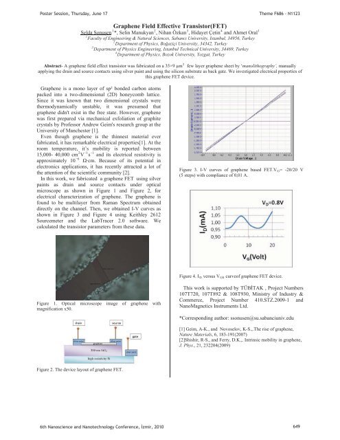
Figure 1. Optical microscope image of graphene with<br />
magnification x50.<br />
This work is supported by TÜBTAK , Project Numbers<br />
107T720, 107T892 & 108T930, Ministry of Industry &<br />
Commerce, Project Number 410.STZ.2009-1 and<br />
NanoMagnetics Instruments Ltd.<br />
*Corresponding author: ssonusen@su.sabanciuniv.edu<br />
[1] Geim, A-K., and Novoselov, K-S.,.The rise of graphene,<br />
Nature Materials, 6, 183-191(2007)<br />
[2]Shishir, R-S., and Ferry, D.K.,. Intrinsic mobility in graphene,<br />
J. Phys., 21, 232204(2009)<br />
Figure 2. The device layout of graphene FET.<br />
6th Nanoscience and Nanotechnology Conference, zmir, <strong>2010</strong> 649


