

Third Day Poster Session, 17 June 2010 - NanoTR-VI
Third Day Poster Session, 17 June 2010 - NanoTR-VI
Third Day Poster Session, 17 June 2010 - NanoTR-VI

Create successful ePaper yourself
Turn your PDF publications into a flip-book with our unique Google optimized e-Paper software.
<strong>Poster</strong> <strong>Session</strong>, Thursday, <strong>June</strong> <strong>17</strong><br />
Theme F686 - N1123<br />
A New Method: Thickness Determination of Thin Films by Energy Dispersive X-ray<br />
Spectroscopy<br />
Sedat Canli 1,2* , Mustafa Kulakci 3 , Urcan Guler 3 , Rasit Turan 2,3<br />
1 Micro and Nanotechnology Department, Middle East Technical University, 06531 Ankara, Turkey<br />
2 Central Laboratory, Middle East Technical University, 06531 Ankara, Turkey<br />
3 Department of Physics, Middle East Technical University, 06531 Ankara, Turkey<br />
Abstract- EDS is a tool for quantitative and qualitative analysis of the materials. In electron microscopy, the energy of the<br />
electrons determines the depth of the region where the x-rays come from. By varying the energy of the electrons, the depth of<br />
the region where x-rays come from can be changed. Different quantitative ratios of the elements for different electron<br />
energies can be obtained using a thin film. The thickness of a specific film on a specific substrate corresponds to a unique<br />
energy-ratio diagram. In this study, it is shown that thickness of a thin film can be obtained by an appropriate analysis of the<br />
energy-ratio diagram of the EDS data obtained from the film.<br />
Scanning Electron Microscopes (SEM) and Energy<br />
Dispersive X-ray Spectroscopy (EDS) methods are<br />
being widely used in materials and nanotechnology<br />
researches. Thin films are very important for several<br />
industries, such as electronic semiconductor industry,<br />
optical coating industry or photovoltaic cells. In the<br />
current work, EDS was investigated as a potential tool<br />
to be used as a relatively easy methodology for<br />
measuring the thickness of thin films.<br />
Silicon, the main material of semiconductor<br />
technology was used as the substrate in this study.<br />
Gold, germanium and aluminum were coated on<br />
substrates by thermal evaporation method and SiO 2 was<br />
grown by the wet oxidation method. Corroborative<br />
thickness measurements were obtained by profilometer<br />
and ellipsometry.<br />
It is known that the electron beam generated by an<br />
SEM hits perpendicularly onto the surface of the films<br />
and the interaction volume changes with the applied<br />
electron energy. In the present study, energy values in<br />
the range of 3keV to 30keV with steps of 1keV were<br />
used.<br />
Figure 1: Monte Carlo electron trajectory simulations of the<br />
interaction volume in Fe at (a) 10keV. (b) 20keV. (c) 30keV [1].<br />
At atomic scale, focused electrons hitting the sample<br />
excite inner electrons of the atoms. During the<br />
relaxation of the atoms, each atom radiates<br />
characteristic x-rays from K α , K β , L α , etc shells [2]. The<br />
detector collects and counts x-rays coming from the<br />
sample and constructs the spectrum. The EDS system<br />
normalizes and corrects the data using ZAF<br />
coefficients, and finally gives ratios of the elements.<br />
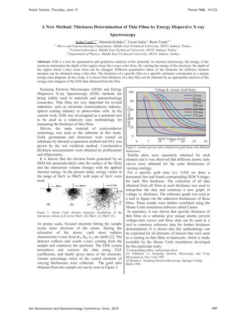
Atomic percentage ratios of the coated elements of<br />
varying thicknesses were collected. The gold ratio<br />
obtained from this sample set can be seen in Figure 2.<br />
Gold Ratio (%)<br />
100<br />
80<br />
60<br />
40<br />
20<br />
0<br />
Voltage & Atomic Gold Ratio<br />
25 nm<br />
50 nm<br />
75 nm<br />
100 nm<br />
125 nm<br />
150 nm<br />
<strong>17</strong>5 nm<br />
SEM Voltage (keV)<br />
0 5 10 15 20 25 30<br />
Figure 2: Atomic percent ratios obtained on gold films with different<br />
thicknesses.<br />
Similar plots were separately obtained for each<br />
element and it was observed that different atomic ratio<br />
curves were obtained for the same thicknesses of<br />
varying coatings.<br />
For a specific gold ratio (i.e. %50) we draw a<br />
horizontal line and found corresponding SEM Voltage,<br />
for each film thickness. The collection of all data<br />
obtained from all films at each thickness was used to<br />
interpolate the data and construct a new graph of<br />
voltage vs. thickness. The reference graph was used as<br />
a tool to figure out the unknown thicknesses of these<br />
films. These results were further correlated using the<br />
Monte Carlo simulation software called Casino.<br />
In summary, it was shown that specific thickness of<br />
thin films on a substrate give unique atomic percent<br />
voltage-ratio curves and these data can be used as a<br />
tool to construct reference data for further thickness<br />
determination. It is shown that this methodology can<br />
be exploited for all elements of interest that were used<br />
as a coating on thin films at nanoscale, which is made<br />
available by the Monte Carlo simulations developed<br />
for this particular study.<br />
* Corresponding author: canli@metu.edu.tr<br />
[1] Goldstein J.I. Scanning Electron Microscopy and X-ray<br />
Microanalysis, New York 1992<br />
[2] Reimer L. Scanning Electron Microscopy, Springer-Verlag,<br />
Berlin 1998<br />
6th Nanoscience and Nanotechnology Conference, zmir, <strong>2010</strong> 660


