

Photonic crystals in biology
Photonic crystals in biology
Photonic crystals in biology

You also want an ePaper? Increase the reach of your titles
YUMPU automatically turns print PDFs into web optimized ePapers that Google loves.
Poster Session, Tuesday, June 15<br />
Theme A1 - B702<br />
Structural and electrical properties of spray deposited pure and Sb doped t<strong>in</strong> oxide<br />
* Güven Turgut, Demet Tatar, Serdar Aydın, Erdal Sönmez and Bahatt<strong>in</strong> Düzgün<br />
K. K. Education Faculty, Department of Physics, Ataturk University, Erzurum 25240, Turkey<br />
Abstract— Pure and 2wt. % Sb doped t<strong>in</strong> oxide (SnO 2 :Sb) th<strong>in</strong> films were prepared by spray pyrolysis onto glass substrates at 420 0 C. X-ray<br />
diffraction (XRD) analysis showed that all films are polycrystall<strong>in</strong>e and Sb dop<strong>in</strong>g <strong>in</strong>creased crystall<strong>in</strong>ity. The films are prefentially oriented<br />
along the (110) direction. Atomic force microscopy (AFM) studies showed that roughness (RMS) of 22.52 nm for undoped films has been<br />
slightly reduced to 15.56 nm on Sb dop<strong>in</strong>g films. Hall effect studies have been performed on SnO 2 (TO) and SnO 2 :Sb(ATO) films coated on glass<br />
substrates.The electrical study reveals that the films are degenerate and exhibit n-type electrical conductivityand also Sb dop<strong>in</strong>g <strong>in</strong>creased carrier<br />
concentrarion(n), decreased sheet resistance(Rs) and resistivity(ρ).<br />
Among transparent and conduct<strong>in</strong>g oxides (TCOs), t<strong>in</strong><br />
oxide (TO) is widely used <strong>in</strong> solar cells, display devices,<br />
hybrid microelectronics, stable resistors, touch-sensitive<br />
switches digital displays [1], electro-chromic displays and gas<br />
sensors [2] etc. due to theirs low electrical resistivity, high<br />
optical transmittance <strong>in</strong> visible region, high optical reflectance<br />
<strong>in</strong> <strong>in</strong>frared region, chemically <strong>in</strong>ert and mechanically hard [3].<br />
Many researchers focused on dop<strong>in</strong>g TO, because electrical,<br />
structural and optical properties of TO can be changed by<br />
dop<strong>in</strong>g with F or Sb [1-8].<br />
In this study, pure and 2 wt.% Sb doped SnO 2 th<strong>in</strong> films<br />
onto glass substrates at 420 ο C were deposited by spray<br />
pyrolysis technique. The spray pyrolysis technique is an<br />
attractive method to obta<strong>in</strong> th<strong>in</strong> films because of its simple and<br />
<strong>in</strong>expensive experimental arrangement [9], ease of add<strong>in</strong>g<br />
dop<strong>in</strong>g materials, reproducibility [3], high growth rate and<br />
mass production capability for uniform large area coat<strong>in</strong>gs [7].<br />
We <strong>in</strong>vestigated structural, morphological and electrical<br />
properties of pure and Sb doped SnO 2 th<strong>in</strong> films.<br />
The structural characterization of the films was carried out<br />
by X-ray diffraction (XRD) measurements us<strong>in</strong>g a Rigaku<br />
D/Max-IIIC diffractometer (λ=1.5418Å for CuKα radiation) at<br />
30 kV, 10 mA. Surface morphology was exam<strong>in</strong>ed by atomic<br />
force microscopy (AFM, which was produced by<br />
Nanomagnetics- Instrument). The electrical measurements<br />
were carried out by Hall measurements <strong>in</strong> van der Pauw<br />
configuration.<br />
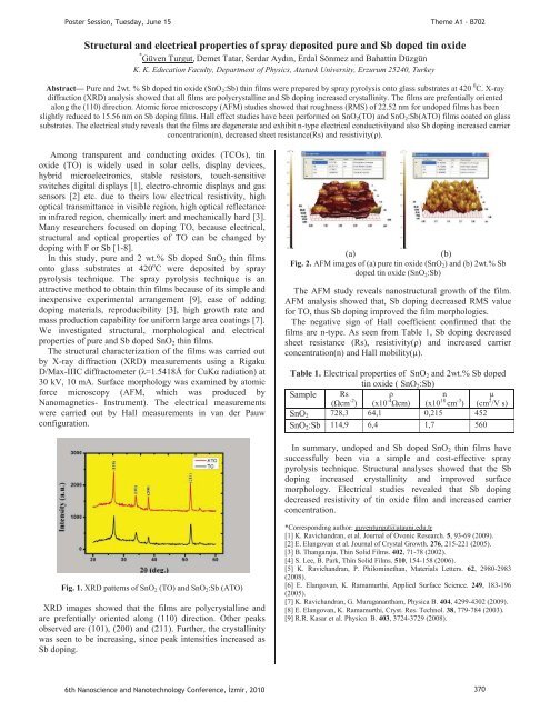
(a)<br />
(b)<br />
Fig. 2. AFM images of (a) pure t<strong>in</strong> oxide (SnO 2 ) and (b) 2wt.% Sb<br />
doped t<strong>in</strong> oxide (SnO 2 :Sb)<br />
The AFM study reveals nanostructural growth of the film.<br />
AFM analysis showed that, Sb dop<strong>in</strong>g decreased RMS value<br />
for TO, thus Sb dop<strong>in</strong>g improved the film morphologies.<br />
The negative sign of Hall coefficient confirmed that the<br />
films are n-type. As seen from Table 1, Sb dop<strong>in</strong>g decreased<br />
sheet resistance (Rs), resistivity(ρ) and <strong>in</strong>creased carrier<br />
concentration(n) and Hall mobility(μ).<br />
Table 1. Electrical properties of SnO 2 and 2wt.% Sb doped<br />
t<strong>in</strong> oxide ( SnO 2 :Sb)<br />
Sample Rs<br />
(Ωcm -2 )<br />
ρ<br />
(x10 -4 Ωcm)<br />
n<br />
(x10 18 cm -3 )<br />
μ<br />
(cm 2 /V s)<br />
SnO 2 728,3 64,1 0,215 452<br />
SnO 2 :Sb 114,9 6,4 1,7 560<br />
In summary, undoped and Sb doped SnO 2 th<strong>in</strong> films have<br />
successfully been via a simple and cost-effective spray<br />
pyrolysis technique. Structural analyses showed that the Sb<br />
dop<strong>in</strong>g <strong>in</strong>creased crystall<strong>in</strong>ity and improved surface<br />
morphology. Electrical studies revealed that Sb dop<strong>in</strong>g<br />
decreased resistivity of t<strong>in</strong> oxide film and <strong>in</strong>creased carrier<br />
concentration.<br />
Fig. 1. XRD patterns of SnO 2 (TO) and SnO 2 :Sb (ATO)<br />
XRD images showed that the films are polycrystall<strong>in</strong>e and<br />
are prefentially oriented along (110) direction. Other peaks<br />
observed are (101), (200) and (211). Further, the crystall<strong>in</strong>ity<br />
was seen to be <strong>in</strong>creas<strong>in</strong>g, s<strong>in</strong>ce peak <strong>in</strong>tensities <strong>in</strong>creased as<br />
Sb dop<strong>in</strong>g.<br />
*Correspond<strong>in</strong>g author: guventurgut@atauni.edu.tr<br />
[1] K. Ravichandran, et al. Journal of Ovonic Research. 5, 93-69 (2009).<br />
[2] E. Elangovan et al. Journal of Crystal Growth. 276, 215-221 (2005).<br />
[3] B. Thangaraju, Th<strong>in</strong> Solid Films. 402, 71-78 (2002).<br />
[4] S. Lee, B. Park, Th<strong>in</strong> Solid Films. 510, 154-158 (2006).<br />
[5] K. Ravichandran, P. Philom<strong>in</strong>ethan, Materials Letters. 62, 2980-2983<br />
(2008).<br />
[6] E. Elangovan, K. Ramamurthi, Applied Surface Science. 249, 183-196<br />
(2005).<br />
[7] K. Ravichandran, G. Muruganantham, Physica B. 404, 4299-4302 (2009).<br />
[8] E. Elangovan, K. Ramamurthi, Cryst. Res. Technol. 38, 779-784 (2003).<br />
[9] R.R. Kasar et al. Physica B. 403, 3724-3729 (2008).<br />
6th Nanoscience and Nanotechnology Conference, zmir, 2010 370


