

Photonic crystals in biology
Photonic crystals in biology
Photonic crystals in biology

You also want an ePaper? Increase the reach of your titles
YUMPU automatically turns print PDFs into web optimized ePapers that Google loves.
Poster Session, Tuesday, June 15<br />
Theme A1 - B702<br />
Synthesis of ZnO Nanowires and Nanorods<br />
Sadullah Öztürk 1 , 1 , 1, Zafer Ziya Öztürk 1 *<br />
1 Gebze Institute of Technology, Science Faculty, Department of Physics, Kocaeli 41400, Turkey<br />
Abstract-In this study, fabrication of ZnO nanostructures such as nanowires and nanorods will be expla<strong>in</strong>ed <strong>in</strong> details. ZnO nanowires were<br />
grown by cathodically <strong>in</strong>duced sol-gel deposition us<strong>in</strong>g an anodic alum<strong>in</strong>um oxide (AAO) template which is approximately 70 nm diameter and<br />
10 μm length. So vertically aligned ZnO nanowires were grown <strong>in</strong> AAO template by apply<strong>in</strong>g cathodic voltage <strong>in</strong> aqueous Z<strong>in</strong>c Nitrate solution<br />
at 23 ºC. For electrochemical deposition, three-electrode system was used. The ZnO nanowires are approximately 65 nm diameter and 10 μm<br />
lengths. For fabrication of ZnO nanorods hydrothermal technique was used. Firstly sol-gel ZnO solution was coated on glass substrate by sp<strong>in</strong><br />
coat<strong>in</strong>g for seed layer. Then ZnO nanorods were grown <strong>in</strong> Z<strong>in</strong>c nitrate and HMTA aqueous solution at 90 ºC about 3h. The ZnO nanorods are<br />
approximately 40 nm diameter. The vertical nanowires and nanorods were characterized by scann<strong>in</strong>g electron microscope (SEM).<br />
ZnO nanostructures are attractive material <strong>in</strong> last decade<br />
because of their n-type semiconduct<strong>in</strong>g behavior with large<br />
exciton b<strong>in</strong>d<strong>in</strong>g energy (60 meV) and a large band gap (3.37<br />
eV). ZnO nanostructures can be used <strong>in</strong> novel devices, such as<br />
photonic devices and very sensitive chemical sensors etc. In<br />
literature, there are many techniques for fabricat<strong>in</strong>g of ZnO<br />
nanowires such as electrochemical and chemical vapor<br />
deposition, and also for fabrication ZnO nanorods such as<br />
hydrothermal, sonochemical and chemical vapor deposition<br />
technique [1,2]. In this study, ZnO nanowires were grown <strong>in</strong><br />
an AAO template with 75 nm diameter and m <strong>in</strong> length by<br />
electrochemical deposition techniques. The AAO template<br />
was grown on Al foil with two anodization techniques and the<br />
details were given [1]. ZnO nanowires were electrodeposited<br />
<strong>in</strong> this template with apply<strong>in</strong>g -1.5V at room temperature<br />
about 2h. Then AAO template was etched <strong>in</strong> NaOH aqueous<br />
solution. So ZnO nanowires was obta<strong>in</strong>ed with 70 nm<br />
ZnO nanowires was shown <strong>in</strong><br />
figure 1.<br />
On the other hand for prepar<strong>in</strong>g ZnO nanorods, ZnO seed<br />
layer solution was deposited on glass with sp<strong>in</strong> coat<strong>in</strong>g at<br />
2500 rpm about 30s. Then the coated glass was dried <strong>in</strong> an<br />
oven at 130°C for 5m<strong>in</strong>. and this step was repeated 5 times.<br />
F<strong>in</strong>ally, ZnO seed layer glass was annealed 300 °C<br />
approximately 1h. The ZnO nanorods were grown <strong>in</strong><br />
Zn(NO 3 ) 2 .6H 2 O and HMTA equmolar aqueous solution at<br />
90 °C about 3h on ZnO seed layer coated glass. For prepar<strong>in</strong>g<br />
of nanorods, cleavable laboratory bottle was used. ZnO seed<br />
layer coated glass was put <strong>in</strong> vertically. ZnO nanorods were<br />
40nm diameter and 800nm length. ZnO nanorods were shown<br />
<strong>in</strong> Figure 2<br />
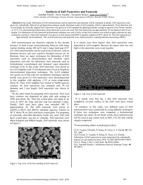
It is clearly seen from figure1 that, ZnO nanowires were<br />
deposited <strong>in</strong> AAO template. Because the aspect ratio was very<br />
high so the nanowires were come together.<br />
Figure 2. Top view of ZnO nanorods<br />
It is clearly seen fron fig. 2 that ZnO nanorods were<br />
completely covered surface of the ZnO seed layer coated<br />
glass.<br />
In summary, <strong>in</strong> this study, two different types of ZnO<br />
nanostructures were synthesized by us<strong>in</strong>g different techniques.<br />
If these two techniques were compared, a hydrothermal<br />
technique was easier. In our future works, these nanostructures<br />
will be used as gas sensor such as NO2, CO, H2 and volatile<br />
organic compound.<br />
*Correspond<strong>in</strong>g author: zozturk@gyte.edu.tr<br />
[1] N. Tüüzer, Z. Z. Öztürk, 95, 781-<br />
787, 2009<br />
[2] S. Öüzer, Z.Z. Öztürk,<br />
Fabrication of ZnO nanowires at room temperature by cathodically<br />
<strong>in</strong>duced sol–gel method <strong>in</strong> press, DOI: 10.1007/s00339-009-5504-8<br />
[3] Z.L. Wang, J. Phys: Cond. Matt. 16, R829 (2004).<br />
[4] L. Schmidt-Mende, J. MacManus-Driscoll, Materials Today, 10,<br />
40 (2007).<br />
Figure 1. Top view of the free stand<strong>in</strong>g of ZnO nanowire<br />
6th Nanoscience and Nanotechnology Conference, zmir, 2010 403


