

Photonic crystals in biology
Photonic crystals in biology
Photonic crystals in biology

Create successful ePaper yourself
Turn your PDF publications into a flip-book with our unique Google optimized e-Paper software.
Poster Session, Tuesday, June 15<br />
Theme A1 - B702<br />
Preparation of z<strong>in</strong>c nitride (Zn 3 N 2 ) nanopowders and their optical properties.<br />
Waheed S. Khan * , Chuanbao Cao<br />
Research Center of Materials Science, Beij<strong>in</strong>g Institute of Technology, Beij<strong>in</strong>g 100081, P. R. Ch<strong>in</strong>a<br />
Abstract- Z<strong>in</strong>c nitride (Zn 3 N 2 ) nanopowders were prepared by nitridation of aqueous ammonia treated z<strong>in</strong>c precursor under ammonia<br />
gas reaction (150 sccm) at 600 o C for 120 m<strong>in</strong>utes <strong>in</strong>side horizontal tube (HT) furnace. The as-prepared product was characterized by<br />
XRD, scann<strong>in</strong>g electron microscopy (SEM) and energy dispersive x-ray spectroscopy (EDS). Us<strong>in</strong>g Scherrer formula, particles size of<br />
nanopowders was found to be 40-50 nm. Room temperature photolum<strong>in</strong>escence (PL) spectrum exhibited a broad ultraviolet (UV)<br />
emission band at 389 nm correspond<strong>in</strong>g to near band edge emission of z<strong>in</strong>c nitride. These studies <strong>in</strong>dicated the potential of the z<strong>in</strong>c nitride<br />
for applications <strong>in</strong> the UV-light emitt<strong>in</strong>g devices.<br />
Over the past few years, z<strong>in</strong>c nitride (Zn 3 N 2 ) has attracted<br />
much research focus due to its n-type conduction, high<br />
electron mobility of about 100 cm 2 V -1 s -1 at room<br />
temperature [1], wide band gap of 3.2 eV [2-3] and its use as<br />
channel layer <strong>in</strong> TTFTs [4]. The other most important aspect<br />
associated with z<strong>in</strong>c nitride is its conversion <strong>in</strong>to p-type ZnO<br />
[5]. The band gap of z<strong>in</strong>c nitride has been a controversial<br />
issue as it has no s<strong>in</strong>gle agreed value but different values<br />
rang<strong>in</strong>g from 0.9 eV [6] to 3.2 eV [2]. One ma<strong>in</strong> reason of<br />
this variation is different preparative routes of z<strong>in</strong>c nitride.<br />
Practical applications of Zn 3 N 2 demand the resolution of this<br />
controversy. It is comparatively a new material and<br />
researchers have started explor<strong>in</strong>g its electronic, optical and<br />
electrical properties s<strong>in</strong>ce 1993. Most of the stress on z<strong>in</strong>c<br />
nitride work has been on its th<strong>in</strong> film/polycrystall<strong>in</strong>e structure<br />
and few reports can be found on nanostructured z<strong>in</strong>c nitride<br />
[3, 7].<br />
In the present work, we report the synthesis,<br />
characterization and optical properties of Zn 3 N 2. About 2<br />
gram z<strong>in</strong>c powder (99.9%) mixed with aqueous ammonia was<br />
loaded <strong>in</strong> alum<strong>in</strong>a boat and shifted to the centre of the<br />
horizontal tube (HT) furnace. The precursor was heated at<br />
600 o C for 2h under NH 3 gas flow of 150 sccm. A black color<br />
product was obta<strong>in</strong>ed <strong>in</strong> the boat on cool<strong>in</strong>g to room<br />
temperature. The crystal structure and phase purity were<br />
tested by XRD analysis. All the diffraction peaks <strong>in</strong> XRD<br />
spectrum of black powder were <strong>in</strong>dexed to the cubic<br />
structured z<strong>in</strong>c nitride (Zn 2 N 3 ) with lattice parameter a=0.976<br />
nm match<strong>in</strong>g very well with that given <strong>in</strong> JCPDS data (Card<br />
No. 035-0762). No other phase like Zn, ZnO was observed <strong>in</strong><br />
the product. The particle size of z<strong>in</strong>c nitride nanopowders<br />
was calculated by us<strong>in</strong>g Scherrer‘s equation with the help of<br />
XRD data. Energy dispersive x-ray spectroscopy (EDS)<br />
exhibited the presence of z<strong>in</strong>c and nitrogen <strong>in</strong> the product. A<br />
small peak of oxygen was also observed <strong>in</strong> EDS possibly due<br />
to the <strong>in</strong>clusion of oxygen on the surface while measurement<br />
procedure.<br />
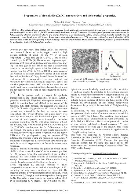
Figure (a) presents SEM image of a particular portion of z<strong>in</strong>c<br />
nitride product prepared at 600 o C under ammonia gas flow<br />
for 120 m<strong>in</strong>utes. From SEM micrographs, it can be clearly<br />
observed that z<strong>in</strong>c nitride consists of nanoparticles with<br />
average dimensions much less than 100 nm which is very<br />
close to the values calculated by Scherrer formula.<br />
Room temperature PL emission spectrum of Zn 3 N 2<br />
nanopowders measured at an excitation wavelength of 325<br />
nm us<strong>in</strong>g Xe lamp source is shown <strong>in</strong> Figure (b). The<br />
spectrum exhibits a very prom<strong>in</strong>ent and broad peak at 389 nm<br />
<strong>in</strong> ultraviolet (UV) region which corresponds to band gap of<br />
Zn 3 N 2 . This value is very close to the reported values of 3.2<br />
eV [2, 3] estimated by PL spectra. The UV band at 389 nm<br />
Figure: (a) SEM image of z<strong>in</strong>c nitride nanopowders. (b) Room<br />
temperature PL spectrum of Zn 3 N 2 product.<br />
rig<strong>in</strong>ates from near band-edge transition of cubic z<strong>in</strong>c nitride<br />
[3] and can possibly be attributed to the excitonic emission<br />
caused by radiative recomb<strong>in</strong>ation of electrons and holes [8].<br />
The absence of the emission bands <strong>in</strong> the visible region<br />
<strong>in</strong>dicate the non-existence of defects and hence purity of the<br />
product. PL <strong>in</strong>vestigations of z<strong>in</strong>c nitride nanopowders<br />
demonstrate the promise of the material for UV-light emitt<strong>in</strong>g<br />
devices.<br />
In conclusion, we have successfully synthesized Zn 3 N 2<br />
nanopowders via nitridation of aqueous ammonia mixed z<strong>in</strong>c<br />
source at 600 o C for 2 hours. The structural, compositional<br />
and morphological characterizations were performed by<br />
XRD, EDS and SEM tests. The room temperature PL studies<br />
of z<strong>in</strong>c nitride exhibited a broad emission UV band<br />
correspond<strong>in</strong>g to the band gap of the product. This feature<br />
<strong>in</strong>dicates the promise of the z<strong>in</strong>c nitride for applications <strong>in</strong><br />
UV-light emitt<strong>in</strong>g devices.<br />
This work was supported by National Natural Science<br />
Foundation of Ch<strong>in</strong>a ((20471007). We are thankful to Higher<br />
Education Commission (HEC) Pakistan for provid<strong>in</strong>g<br />
f<strong>in</strong>ancial support for present<strong>in</strong>g this paper <strong>in</strong> the 6th<br />
Nanoscience and Nanotechnology Conference (NanoTR6-<br />
2010) held <strong>in</strong> Turkey.<br />
*Correspond<strong>in</strong>g author: waheedskhan@yahoo.com<br />
[1] Futsuhara, M., Yoshioka, K. and Takai, O., Futsuhara, M., 1998.<br />
Th<strong>in</strong> Solid Films 322: 274 .<br />
[2] Kuriyama, K., Takahashi, Y., Sunohara, F.,1993. Phys. Rev. B<br />
48: 2781.<br />
[3] Zong, F., et al., 2005. Appl. Phys. Lett. 87: 233104.<br />
[4] Aperathitis, E., et al., 2009. Th<strong>in</strong> Solid Films 518: 1036.<br />
[5] Kambilafka, V., et al., 2007. Superlattices Microstruct. 42: 55.<br />
[6] Paniconi, G., et al., 2008. J. Solid State Chem. 181: 158.<br />
[7] Waheed S. Khan, Chuanbao Cao, 2010. J. Crys. Growth (In<br />
press).<br />
[8] Kam<strong>in</strong>ska, E., et al., 2005. Phys. Status Solidi (c) 2: 1119.<br />
6th Nanoscience and Nanotechnology Conference, zmir, 2010 228


