

Photonic crystals in biology
Photonic crystals in biology
Photonic crystals in biology

You also want an ePaper? Increase the reach of your titles
YUMPU automatically turns print PDFs into web optimized ePapers that Google loves.
Poster Session, Tuesday, June 15<br />
Theme A1 - B702<br />
Effect of defects on the radiat ion sensitivity o f PECVD Ge doped amorphous SiO x<br />
Sedat A 1 , 1 1 2<br />
1 TURKEY<br />
2 Department of Physics, <br />
Abstract- In this study, optical properties of Ge nano<strong>crystals</strong> <strong>in</strong> SiOx structures are <strong>in</strong>vestigated by us<strong>in</strong>g Raman, photolum<strong>in</strong>escence<br />
spectroscopy and electron sp<strong>in</strong> resonans (ESR) techniques. Ge nanocrystal <strong>in</strong> silicon oxide th<strong>in</strong> films have been grown with different flow<br />
rate of GeH 4 , SiH 4 and N 2 O by plazma enhanced chemical vapor deposition (PECVD) technique. We report experimental <strong>in</strong>vestigation by<br />
ESR measurements of room temperature -ray irradiation effects <strong>in</strong> PECVD Ge doped amorphous SiO x .<br />
Electronically active defects have a very significant<br />
<strong>in</strong>fluence on the electronic transport and optical properties,<br />
lead<strong>in</strong>g to compensation effects or to fast nonradiative<br />
recomb<strong>in</strong>ation. Ge-related defects that are cause of<br />
attenuation for the waveguides, thus lead<strong>in</strong>g to detrimental<br />
losses of part of the transmitted signals [1-2]. The<br />
identification of the specific defects, sensitive to radiation,<br />
is therefore of crucial importance to make clear the<br />
microscopic orig<strong>in</strong> of technologically relevant processes.<br />
Various experiments have shown that this defect centre<br />
can be produced by either two-photon absorption of<br />
excimer laser light (KrF, XeCl or ArF), s<strong>in</strong>gle-photon<br />
absorption of light from a KrCl excimer lamp [3] or by<br />
ioniz<strong>in</strong>g radiation such as x- or -rays. In the <strong>in</strong>teraction of<br />
radiation with Ge-doped silica new defects are <strong>in</strong>duced.<br />
These defect centers are usually named Ge-related<br />
paramagnetic po<strong>in</strong>t defects (GECs).<br />
Electron paramagnetic Resonance (EPR), one of the<br />
most powerful techniques for determ<strong>in</strong><strong>in</strong>g po<strong>in</strong>t defects <strong>in</strong><br />
semiconduct<strong>in</strong>g <strong>crystals</strong>. The aim of our work is to<br />
determ<strong>in</strong>e the paramagnetic po<strong>in</strong>t defects as well as the<br />
defect concentration <strong>in</strong> the gamma ray irradiation with<br />
annealed and as-grown germano-silicate PECVD grown<br />
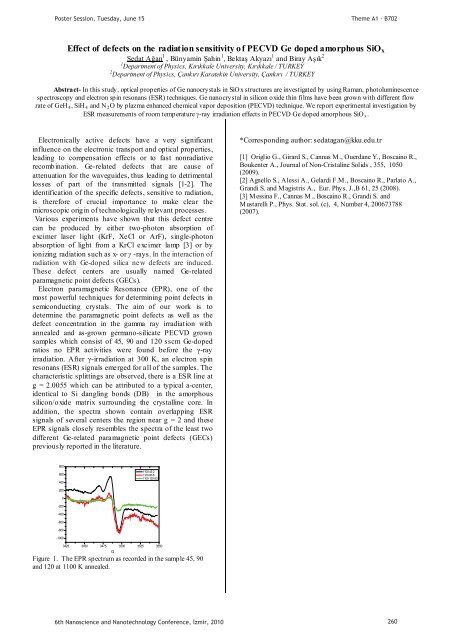
samples which consist of 45, 90 and 120 sscm Ge-doped<br />
ratios no EPR activities were found before the -ray<br />
irradiation. After -irradiation at 300 K, an electron sp<strong>in</strong><br />
resonans (ESR) signals emerged for all of the samples. The<br />
characteristic splitt<strong>in</strong>gs are observed, there is a ESR l<strong>in</strong>e at<br />
g = 2.0055 which can be attributed to a typical a-center,<br />
identical to Si dangl<strong>in</strong>g bonds (DB) <strong>in</strong> the amorphous<br />
silicon/o xide matrix surround<strong>in</strong>g the crystall<strong>in</strong>e core. In<br />
addition, the spectra shown conta<strong>in</strong> overlapp<strong>in</strong>g ESR<br />
signals of several centers the region near g = 2 and these<br />
EPR signals closely resembles the spectra of the least two<br />
different Ge-related paramagnetic po<strong>in</strong>t defects (GECs)<br />
previously reported <strong>in</strong> the literature.<br />
*Correspond<strong>in</strong>g author: sedatagan@kku.edu.tr<br />
[1] Origlio G., Girard S., Cannas M., Ouerdane Y., Bosca<strong>in</strong>o R.,<br />
Boukenter A., Journal of Non-Cristal<strong>in</strong>e Solids , 355, 1050<br />
(2009).<br />
[2] Agnello S., Alessi A., Gelardi F.M., Bosca<strong>in</strong>o R., Parlato A.,<br />
Grandi S. and Magistris A., Eur. Phys. J.,B 61, 25 (2008).<br />
[3] Mess<strong>in</strong>a F., Cannas M., Bosca<strong>in</strong>o R., Grandi S. and<br />
Mustarelli P., Phys. Stat. sol. (c), 4, Number 4, 200673788<br />
(2007).<br />
800<br />
600<br />
400<br />
1100-45-2<br />
1100-90-6<br />
1100-120-0D<br />
200<br />
0<br />
-200<br />
-400<br />
-600<br />
-800<br />
-1000<br />
3425 3450 3475 3500 3525 3550<br />
G<br />
Figure 1. The EPR spectrum as recorded <strong>in</strong> the sample 45, 90<br />
and 120 at 1100 K annealed.<br />
6th Nanoscience and Nanotechnology Conference, zmir, 2010 260


