

Photonic crystals in biology
Photonic crystals in biology
Photonic crystals in biology

Create successful ePaper yourself
Turn your PDF publications into a flip-book with our unique Google optimized e-Paper software.
Poster Session, Tuesday, June 15<br />
Theme A1 - B702<br />
The Effect of the Quantum Po<strong>in</strong>t Contacts and Impurities on an Electron <strong>in</strong> the 2D Electron Gas<br />
Eng<strong>in</strong> Cicek 1 , Mustafa Ulas 2 and Afif Siddiki 3,4<br />
1 Department of Physics, Trakya University, 22030 Edirne, Turkey<br />
2 Kirklareli University, Physics Department, Faculty of Arts and Science, Kavakli-Kirklareli, Turkey<br />
3 Istanbul University, Faculty of Sciences, Physics Department, Vezneciler-Istanbul, 34134, Turkey<br />
4 Harvard University, Physics Department, Cambridge, 02138 MA, USA<br />
Abstract— In this work, we <strong>in</strong>vestigate the geometrical effects of the s<strong>in</strong>gle and double quantum po<strong>in</strong>t contacts (QPCs) and<br />
impurity effects on a two dimensional electron gas (2DEG) <strong>in</strong> the AlGaAs/GaAs heterostructure. For a realistic calculation we<br />
take <strong>in</strong>to account the crystal growth parameters and the sample geometries. Next, we solve the three dimensional Poisson<br />
equation us<strong>in</strong>g the numerical techniques. We show that the QPC’s shape and impurity properties strongly changes the<br />
distribution of the two dimensional electron gas (2DEG) and the subband energies of the electron which is the located <strong>in</strong> the<br />
2DEG.<br />
In the last decade, low-dimensional heterostructure<br />
systems such as th<strong>in</strong> films (2D), wires (1D) and quantum dots<br />
(0D) [1-3] have received a great deal of attention because of<br />
their <strong>in</strong>terest<strong>in</strong>g physical properties [4] and their technological<br />
applications <strong>in</strong> electronic and optical devices. Fabrication<br />
techniques affect the electronic properties of the sample so<br />
that for a realistic calculations the real sample properties are<br />
tak<strong>in</strong>g <strong>in</strong>to account [5].<br />
Here we def<strong>in</strong>e a square unit cell, with a surface pattern<br />
(1.5x1.5 m 2 ) where we process three different techniques<br />
(gate, etch and trench gate def<strong>in</strong>ed) at the each edge of the<br />
sample <strong>in</strong> the same direction with 0.5 m. For gate def<strong>in</strong>ed<br />
samples we applied -1.8 V to the gates on the surface, whereas<br />
for etch def<strong>in</strong>ed samples we etched 62.8 nm from the surface<br />
and for trench gate samples we etch the samples 31.4 nm and<br />
place gates on this plane with a -1.8 V bias. QPCs are located<br />
on the surface with a -1.8 V. The two unlike QPC geometries<br />
(X 2 -X 8 ) are used with three different distances of the QPC’s<br />
tips. A s<strong>in</strong>gle impurity is set <strong>in</strong> the heterostructure at various<br />
positions and distances from the 2DEG. To obta<strong>in</strong> the electron<br />
and potential profiles we solved the electrostatics of the<br />
system <strong>in</strong> three dimensions with us<strong>in</strong>g a code developed on a<br />
fourth order grid, which was successfully applied <strong>in</strong> previous<br />
studies [6,7]. For a realistic calculation we take <strong>in</strong>to account<br />
the crystal growth parameters, gate patterns, surface images,<br />
densities, QPC and impurity properties explicitly. Our results<br />
can enlighten the experimental structures. In our work, 2DEG<br />
is located 314 nm below the surface and we dope the<br />
heterostructures with two donor layers. The upper donor layer<br />
is 40 nm below the surface and its density is 1.7x10 16 m -2 ,<br />
whereas the other donor layer is located 165 nm below the<br />
surface with a fixed dop<strong>in</strong>g surface density of 2.5x10 15 m -2 .<br />
These donor layers are distributed homogeneously. We<br />
compare the electron density distributions and potential<br />
profiles where we create the 2DEG with different techniques<br />
(etch<strong>in</strong>g, gate and trench gated def<strong>in</strong>ed structures), QPC<br />
shapes and impurity positions.<br />
As a result, the edge properties of the 2DEG is strongly<br />
affected by the shape of the QPC, impurity position and the<br />
which process procedure is used. We can solve the 3D Poisson<br />
equation iteratively and take <strong>in</strong>to account these properties and<br />
wafer properties of the sample. So that we obta<strong>in</strong> deep <strong>in</strong>sight<br />
of the realistic samples.<br />
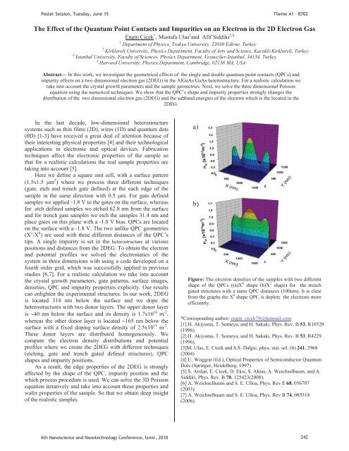
a)<br />
b)<br />
Figure: The electron densities of the samples with two different<br />
shape of the QPCs ((a)X 8 shape (b)X 2 shape) for the trench<br />
gated structures with a same QPC distances (100nm). It is clear<br />
from the graphs the X 8 shape QPC is deplete the electrons more<br />
efficiently.<br />
*Correspond<strong>in</strong>g author: eng<strong>in</strong>_cicek79@hotmail.com<br />
[1] H. Akiyama, T. Someya, and H. Sakaki, Phys. Rev. B 53, R10520<br />
(1996).<br />
[2] H. Akiyama, T. Someya, and H. Sakaki, Phys. Rev. B 53, R4229<br />
(1996).<br />
[3]M. Ulas, E. Cicek and S.S. Dalgic, phys. stat. sol. (b) 241, 2968<br />
(2004)<br />
[4] U. Woggon (Ed.), Optical Properties of Semiconductor Quantum<br />
Dots (Spr<strong>in</strong>ger, Heidelberg, 1997).<br />
[5] S. Arslan, E. Cicek, D. Eksi, S. Aktas, A. Weichselbaum, and A.<br />
Siddiki, Phys. Rev. B 78, 125423(2008).<br />
[6] A. Weichselbaum and S. E. Ulloa, Phys. Rev E 68, 056707<br />
(2003).<br />
[7] A. Weichselbaum and S. E. Ulloa, Phys. Rev B 74, 085318<br />
(2006).<br />
6th Nanoscience and Nanotechnology Conference, zmir, 2010 242


